Semiconductor device

a technology of magnetic resonance imaging and magnetic field, applied in the direction of digital storage, transistors, instruments, etc., can solve the problems of very difficult improvement of dwi characteristics and very worse retention characteristics

Inactive Publication Date: 2005-06-30
DONGBU ELECTRONICS CO LTD
View PDF22 Cites 43 Cited by
  • Summary
  • Abstract
  • Description
  • Claims
  • Application Information

AI Technical Summary

Benefits of technology

[0018] Accordingly, the present invention is directed to an nvSRAM that substantially obviates one or more problems due to limitations and disadvantages of the related art.

Problems solved by technology

However, the improvement of the DWI characteristic is very difficult.
In addition, the thickness of the tunnel oxide layer of the SONOS transistor is very thin(generally 20 Å or so), so that a characteristic of the retention is very worse.

Method used


Image

  • Semiconductor device
  • Semiconductor device
  • Semiconductor device

Examples


Embodiment Construction

[0028] Reference will now be made in detail to the preferred embodiments of the present invention, examples of which are illustrated in the accompanying drawings.

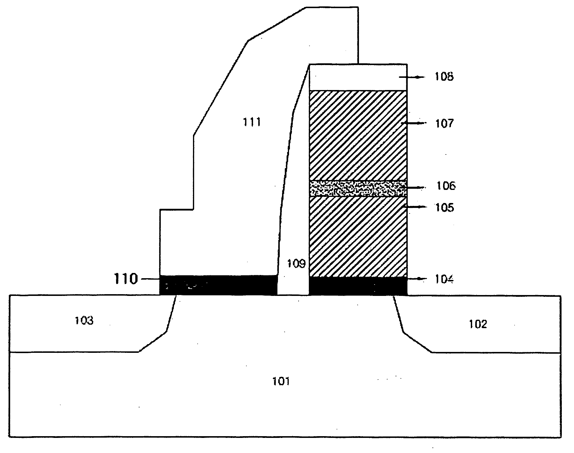
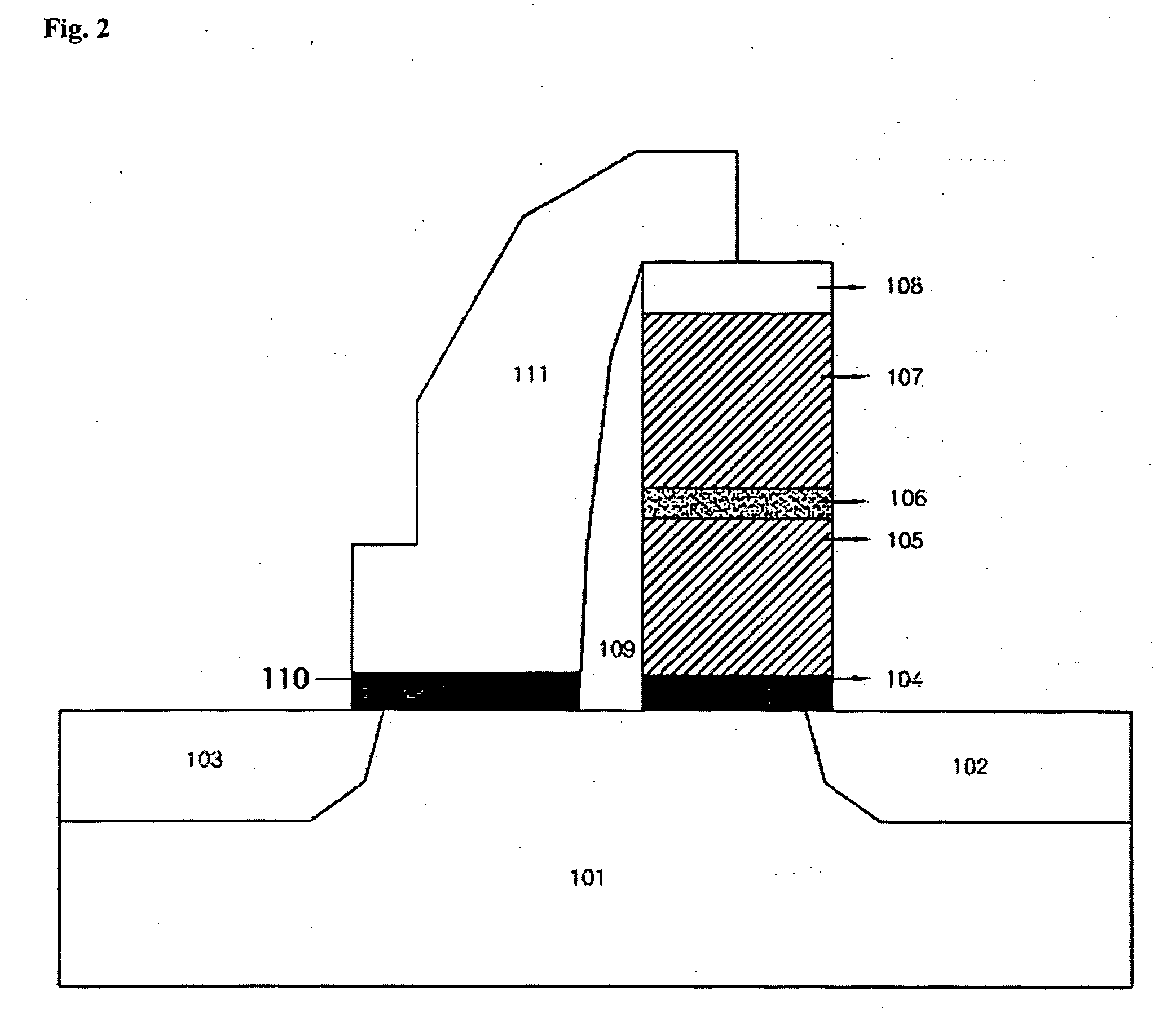
[0029]FIG. 2 is a cross-sectional view illustrating a floating gate NVM device of a split gate structure according to the present invention.

[0030] Referring to FIG. 2, SiO2 is grown on a P-type silicon substrate 101, so that a tunnel oxide layer 104 is completed. A polysilicon floating gate 105, an ONO layer 106 and a control gate 107 are sequentially positioned on the tunnel oxide layer 104. A split gate 111 is located next to a floating gate NVM and a split gate oxide layer 110 is positioned between the split gate 111 and the silicon substrate 101. The floating gate NVM and the split gate 111 are isolated from each other by a first insulation layer 108 and a second insulation layer 109, and a drain 102 and a source 103 are positioned under their sides.

[0031] For the program operation of the device, hot electron injecti...


PUM


Abstract

An nvSRAM having a stacked oxide layer is disclosed. A disclosed device comprises: two NMOS transistors and two PMOS transistors for an SRAM latch; two NMOS pass gates for reading and writing a HIGH condition and a LOW condition that are formed in the SRAM latch; and two floating gate NVM devices of split gate structure for storing the HIGH condition and the LOW condition that are stored in the SRAM latch when the power is off.

Description

BACKGROUND OF THE INVENTION [0001] 1. Field of the Invention [0002] The present invention relates to a nonvolatile static random access memory (hereinafter referred to as “nvSRAM”), more particularly, an nvSRAM having a stacked oxide layer instead of conventional silicon-oxide-nitride-oxide-silicon(hereinafter referred to as “SONOS”) structure. [0003] 2. Background of the Related Art [0004]FIG. 1 is a cross-sectional view illustrating structure of an nvSRAM unit cell using a SONOS device in accordance with the prior art. [0005] The unit cell of the conventional nvSRAM comprises eight negative-channel metal oxide semiconductor(hereinafter referred to as “NMOS”) transistors, two positive-channel metal oxide semiconductor(hereinafter referred to as “PMOS”) transistors and two SONOS transistors. In detail, two NMOS transistors and two PMOS transistors for an SRAM latch, two NMOS pass gates for reading and writing a HIGH condition and a LOW condition that are formed in the SRAM latch, tw...

Claims


Application Information

Patent Timeline
Patent Type & Authority Applications(United States)
IPC IPC(8): G11C11/00G11C14/00G11C16/04H01L21/8244H01L21/8247H01L27/105H01L27/11H01L27/115H01L29/788H01L29/792
CPCG11C14/00G11C16/0466G11C16/0425G11C14/0063H10B69/00
Inventor JUNG, JIN HYO
Owner DONGBU ELECTRONICS CO LTD
Why Eureka
Try Eureka