Optical coupler and electronic equipment using same

Inactive Publication Date: 2005-06-30
SHARP KK
View PDF10 Cites 35 Cited by
  • Summary
  • Abstract
  • Description
  • Claims
  • Application Information

AI Technical Summary

Benefits of technology

[0010] In consideration of the above situations, an object of the present invention is to provide an optical coupler capable of offering excellent environment resistance and high reliability with a simple

Problems solved by technology

However, a practical means to perform resin encapsulating with this structure is not disclosed in JP 2000-173947 A. Generally, resin for use in transfer molding has small particles, which induces a phenomenon of resin leaking from a space of several μm.
Therefore, it is considered to be difficult to realize such a structure stated in JP 2000-173947 A. Moreover, in the case of using a semiconductor optical device with a relatively large size (several mm to several dozen mm square) such as CCDs (Charge Coupled Devices), it is possible to dispose a glass lens on an optical portion.
However, a semiconductor optical device with a small size (several hundred μm square) such as LEDs, which has an extremely small optical portion, needs to use a glass lens that is also extremely small in size, thereby causing problems including: (i) it is difficult to design a lens which can offer optical effects; (ii) it is difficult to manufacture a minute glass lens; and (iii) it is difficult to bond and align the optical portion and the glass lens.
Further, if a glass lens that is larger

Method used


Image

  • Optical coupler and electronic equipment using same
  • Optical coupler and electronic equipment using same
  • Optical coupler and electronic equipment using same

Examples


first embodiment

The First Embodiment

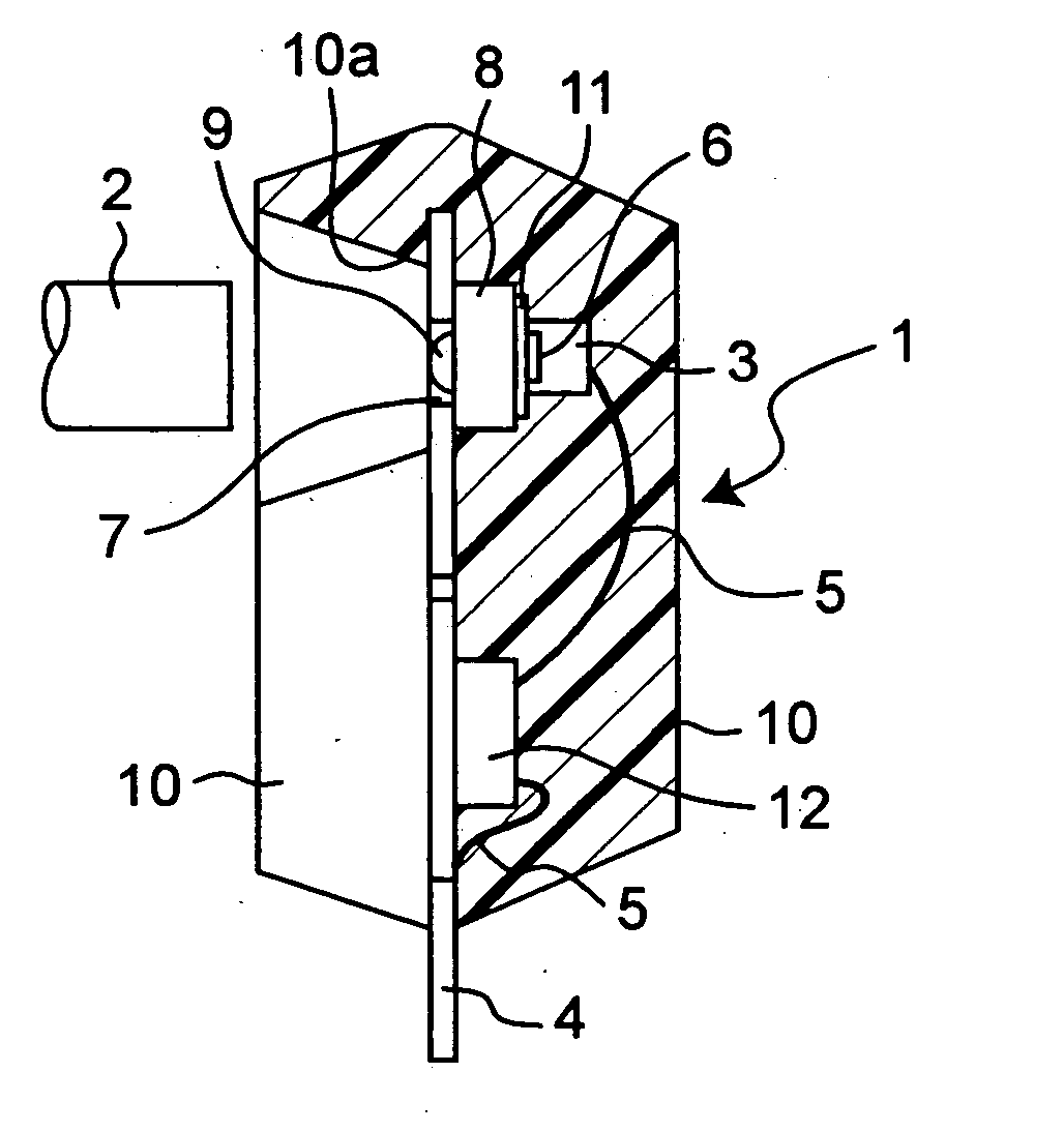
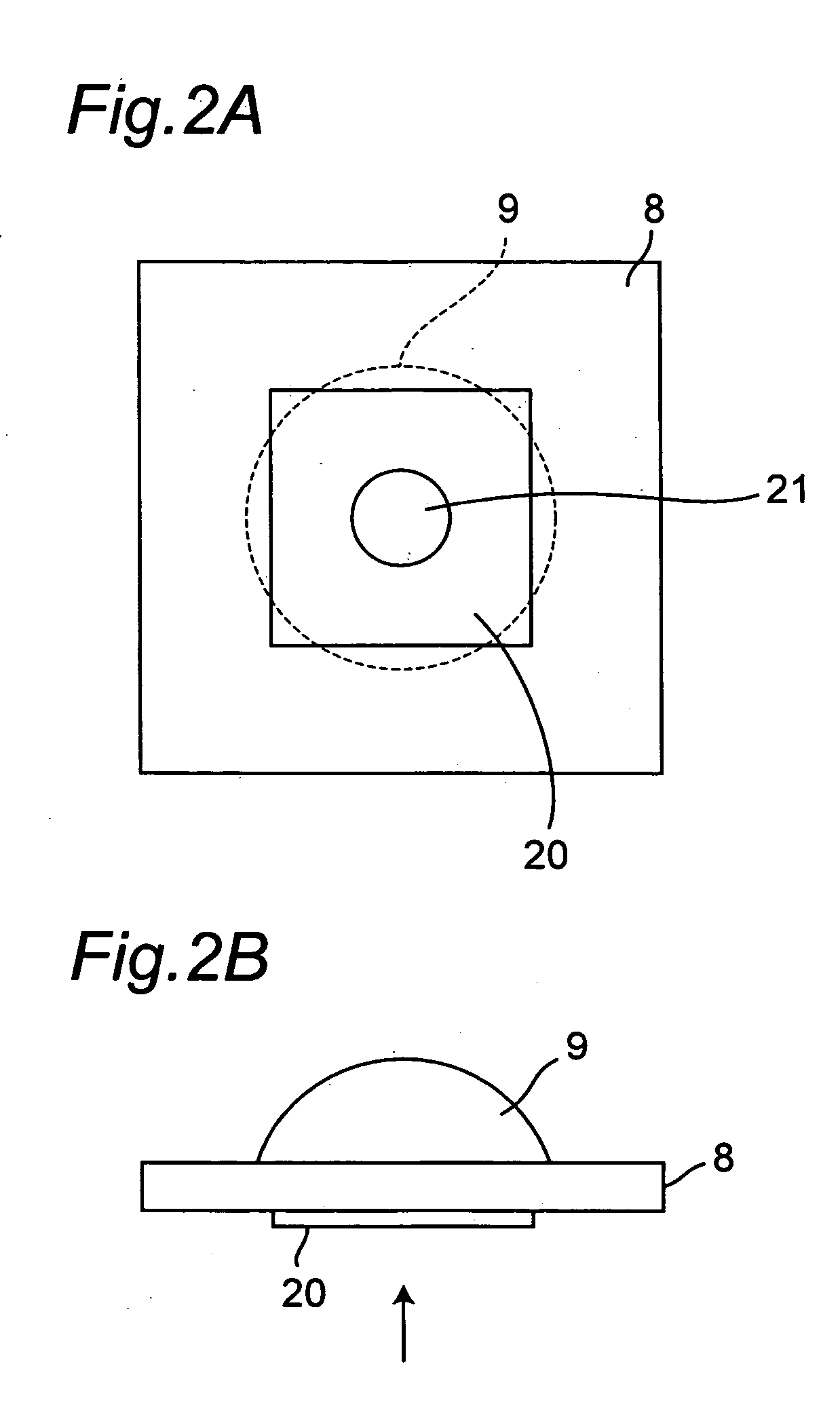
[0066]FIG. 1A is a schematic sectional view showing an outlined structure of an optical coupler according to a first embodiment of the present invention, and FIG. 1B is a front view showing the optical coupler viewed from the side of an optical fiber 2. FIG. 1A shows a section taken along a line I-I of FIG. 1B.

[0067] As shown in FIGS. 1A and 1B, the optical coupler 1 includes a semiconductor optical device 3, a lead frame 4 on which the semiconductor optical device 3 is disposed, a glass submount 8 exemplifying a submount having light transmission, a lens 9 provided on the glass submount 8, and a signal processing circuit (semiconductor device) 12 exemplifying a signal processing integrated circuit. At a position of the lead frame 4 opposed to an optical portion 6 of the semiconductor optical device 3, there is formed an aperture 7 passing through in thickness direction. The optical portion 6 herein refers to a portion for emitting light of the semiconductor opt...

second embodiment

The Second Embodiment

[0097]FIG. 6A is a schematic sectional view showing an outlined structure of an optical coupler according to a second embodiment of the present invention, and FIG. 6B is a front view showing the optical coupler viewed from the side of an optical fiber 2. FIG. 6A shows a section taken along the line VI-VI of FIG. 6B.

[0098] The optical coupler in the second embodiment is different from the optical coupler in the first embodiment of FIGS. 1A and 1B in the point that an IC (Integrated Circuit) 13 is mounted on a glass submount 8, wherein the IC 13 is a single chip incorporating a light-receiving device in the case where the semiconductor optical device is the light-receiving device 3 and an amplifying integrated circuit that is the signal processing circuit 12 in FIGS. 1A and 1B showing the first embodiment.

[0099] The IC 13 formed as a single chip is mounted at the same position as that of the semiconductor optical device 3 in the first embodiment. Other aspects o...

third embodiment

The Third Embodiment

[0102]FIG. 7A is a schematic sectional view showing an outlined structure of an optical coupler according to a third embodiment of the present invention, and FIG. 7B is a front view showing the optical coupler viewed from the side of optical fibers 2. FIG. 7A shows a section taken along the line VII-VII of FIG. 7B.

[0103] The optical coupler in the third embodiment is different from the optical coupler of the first embodiment in the point that a light-emitting device 3b, a light-receiving device 3a, and an IC 14 composed of a driving integrated circuit for the light-emitting device 3b and an amplifying integrated circuit for the light-receiving device 3a are incorporated in a single package. Other aspects are the same as the first embodiment.

[0104] In the optical coupler of the third embodiment, the light-emitting device 3b, the light-receiving device 3a and the IC 14 are incorporated in a single package, which makes it possible to structure an optical coupler f...


PUM


Abstract

On one surface of a lead frame 4 having an aperture 7 passing through in thickness direction thereof, a submount having transparency for closing the aperture 7 of the lead frame 4 is disposed. On a surface of the submount opposite to a surface of the submount 8 facing the aperture 7 of the lead frame 4, a semiconductor optical device 3 is disposed in such a way that an optical portion thereof faces toward the aperture. The semiconductor optical device 3 is electrically connected to the lead frame 4 via wire 5. At least one surface of the lead frame 4, the semiconductor optical device 3 and the submount 8 are encapsulated with a molding portion 10 made of a non-transparent molding resin in a state that the aperture 7 on the other surface side of the lead frame 4 is exposed.

Description

CROSS-REFERENCE TO RELATED APPLICATION [0001] This nonprovisional application claims priority under 35 U.S.C. §119(a) on Patent Application No. 2003-426420 filed in Japan on Dec. 24, 2003, the entire contents of which are hereby incorporated by reference.BACKGROUND OF THE INVENTION [0002] The present invention relates to an optical coupler having a semiconductor optical device and to electronic equipment using the same, and more particularly, relates to an optical coupler for use in optical communication links and so forth for sending and receiving optical signals with an optical fiber as a transmission medium, and electronic equipment using the same. [0003] Conventionally, there have been known optical couplers coupling semiconductor optical devices such as LEDs (Light Emitting Diodes) and PDs (Photo Diodes) to optical fibers, which have been used for optical communications between equipments, at home and in automobiles. [0004] As these optical couplers, those manufactured utilizin...

Claims


Application Information

Patent Timeline
IPC IPC(8): H01L23/29G02B6/00G02B6/42H01L21/00H01L23/31H01L27/14H01L31/00H01L31/02H01L31/167H01L33/48H01L33/54H01L33/56H01L33/62H01S3/08H01S5/00H01S5/022
CPCG02B6/4201G02B6/4204H01L2924/3025H01L2924/01322H01L2224/48247H01L2224/48137H01L2224/48091H01L2224/48257H01L2924/1815H01L2924/19107H01L2924/00014H01L2924/00G02B6/4253G02B6/4255
Inventor OHE, NOBUYUKINAGURA, KAZUHITO
Owner SHARP KK
Why Eureka
Try Eureka