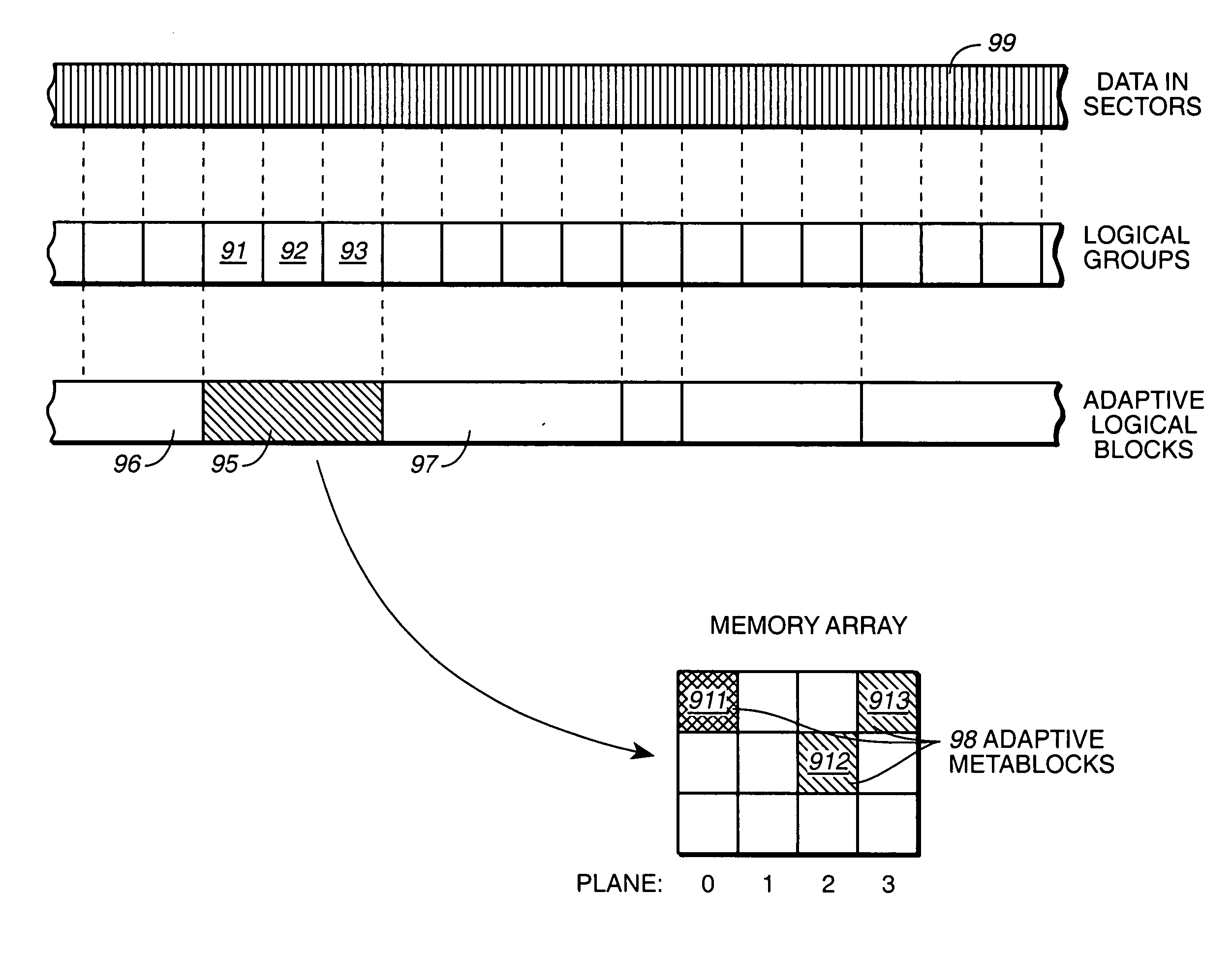
Adaptive metablocks

Active Publication Date: 2005-06-30
SANDISK TECH LLC
View PDF55 Cites 261 Cited by
  • Summary
  • Abstract
  • Description
  • Claims
  • Application Information

AI Technical Summary

Benefits of technology

[0015] Data may be stored in a memory array in adaptive metablocks. The size of an adaptive metablock may be tailored to the data to be stored. Adaptive metablock size may be determined based on the nature of the data

Problems solved by technology

These storage levels do shift as a result of charge disturbing programming, reading or erasing operations performed in neighboring or other related memory cells, pages or blocks.
Also, shifting charge levels can be restored back to the centers of their state ranges from time-to-time, before disturbing operations cause them to shift completely out of their defined ranges and thus cause erroneous data to be read.
Zones are primarily used to simplify address management such as logical to physical translation, resulting in sma

Method used


Image

  • Adaptive metablocks
  • Adaptive metablocks
  • Adaptive metablocks

Examples


Embodiment Construction

Memory Architectures and Their Operation

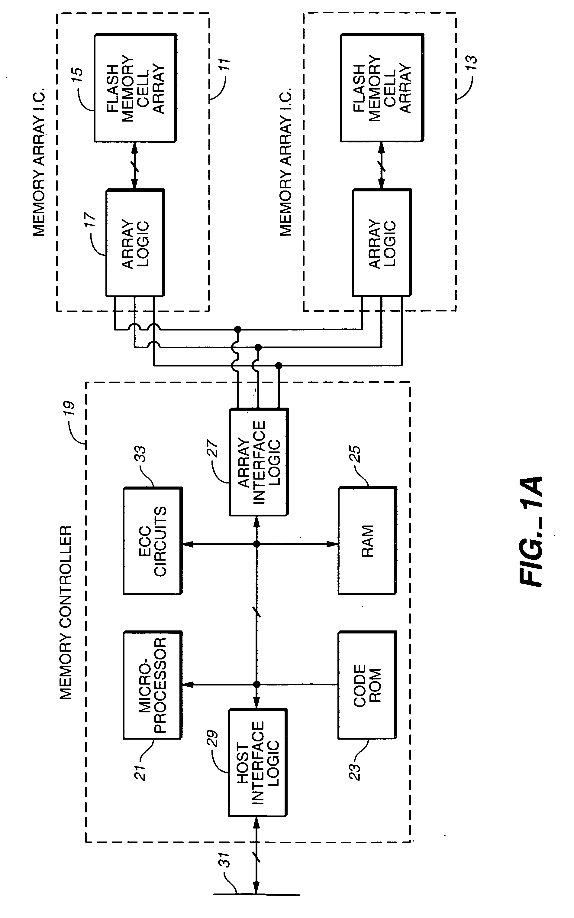
[0050] Referring initially to FIG. 1A, a flash memory includes a memory cell array and a controller. In the example shown, two integrated circuit devices (chips) 11 and 13 include an array 15 of memory cells and various logic circuits 17. The logic circuits 17 interface with a controller 19 on a separate chip through data, command and status circuits, and also provide addressing, data transfer and sensing, and other support to the array 13. A number of memory array chips can be from one to many, depending upon the storage capacity provided. A memory cell array may be located on a single chip or may be comprised of memory cells on multiple chips. The controller and part or the entire array can alternatively be combined onto a single integrated circuit chip but this is currently not an economical alternative.

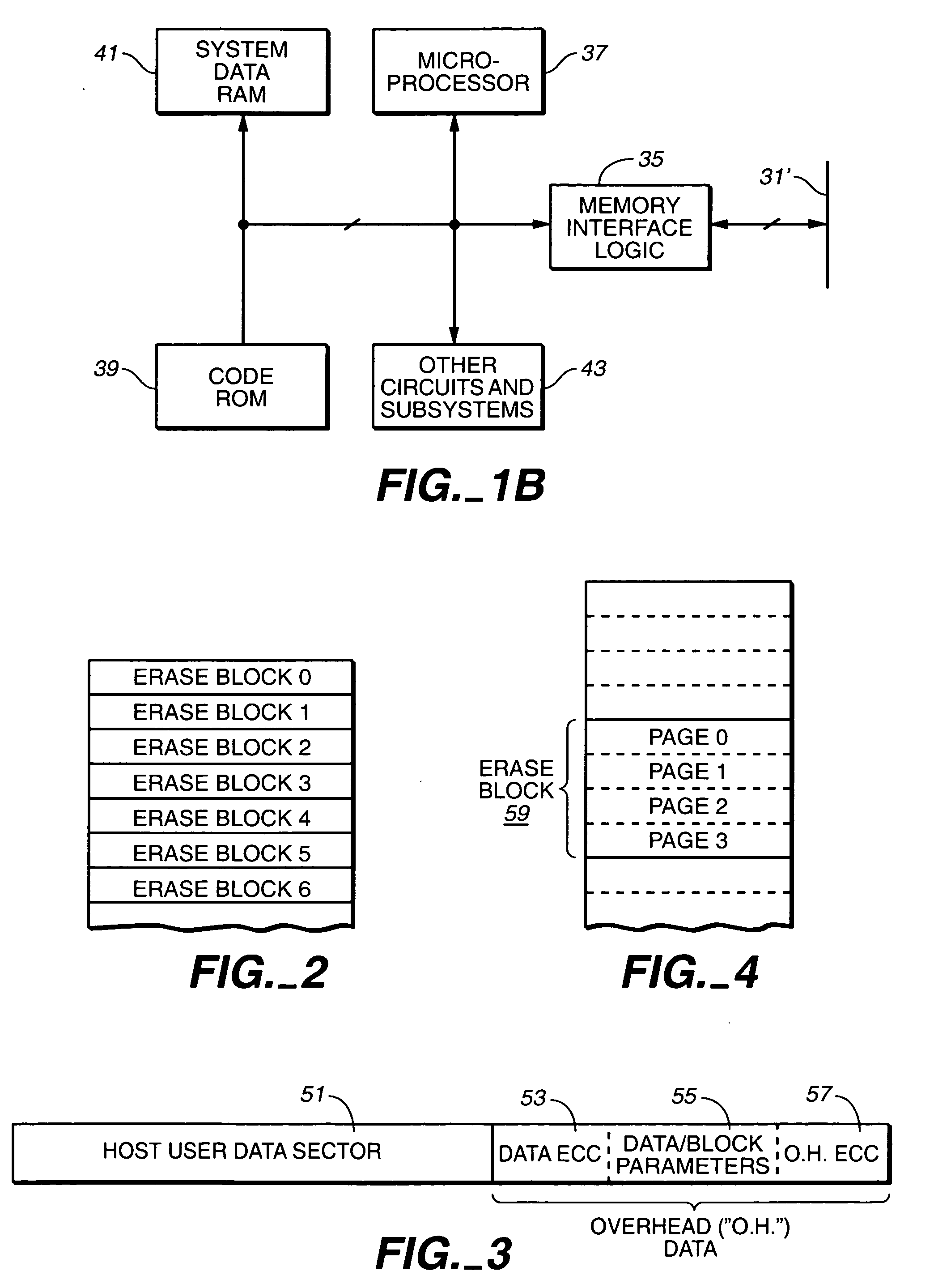
[0051] A typical controller 19 includes a microprocessor 21, a read-only-memory (ROM) 23 primarily to store firmware and a buffer memory...


PUM


Abstract

In a memory system having multiple erase blocks in multiple planes, a selected number of erase blocks are programmed together as an adaptive metablock. The number of erase blocks in an adaptive metablock is chosen according to the data to be programmed. Logical address space is divided into logical groups, a logical group having the same size as one erase block. Adaptive logical blocks are formed from logical groups. One adaptive logical block is stored in one adaptive metablock.

Description

BACKGROUND [0001] This invention relates generally to the operation of non-volatile memory systems, and, more specifically, to the handling of data within such memory systems. [0002] There are many commercially successful non-volatile memory products being used today, particularly in the form of small form factor cards, which employ an array of flash EEPROM (Electrically Erasable and Programmable Read Only Memory) cells formed on one or more integrated circuit chips. A memory controller, usually but not necessarily on a separate integrated circuit chip, interfaces with a host to which the card is removably connected and controls operation of the memory array within the card. Such a controller typically includes a microprocessor, some non-volatile read-only-memory (ROM), a volatile random-access-memory (RAM) and one or more special circuits such as one that calculates an error-correction-code (ECC) from data as they pass through the controller during the programming and reading of da...

Claims


Application Information

Patent Timeline
IPC IPC(8): G06F12/00G06F12/02G06F12/08
CPCG06F12/0246G06F2212/7208G06F2212/7207
Inventor SINCLAIR, ALAN WELSH
Owner SANDISK TECH LLC
Why Eureka
Try Eureka