Amplifiers using gated diodes

a technology of gated diodes and amplifiers, applied in semiconductor devices, solid-state devices, instruments, etc., can solve the problems of circuits sensitive to voltage, temperature and process variations, and difficult control of items, and achieve the effect of preventing voltage ris

Active Publication Date: 2005-07-07
GLOBALFOUNDRIES US INC
View PDF10 Cites 36 Cited by
  • Summary
  • Abstract
  • Description
  • Claims
  • Application Information

AI Technical Summary

Benefits of technology

[0011] A gated diode may be implemented in a number of ways, such as through a device comprising an insulator formed between a gate and a well, a source diffusion region abutting and overlapping one side of the insulator and gate, and a shallow trench isolation region abutting another side of the insulator and gate, wherein the source input is coupled to the source diffusion region and the gate input is coupled to the gate. Additionally, the gated diode could comprise an insulator formed between a gate and a well, a source diffusion region abutting and overlapping one side of the insulator and gate, a drain diffusion region abutting and overlapping another side of the insulator and gate, and a coupling that directly couples the source and drain regions, wherein the source input is coupled to the source diffusion region and the gate input is coupled to the gate. The gated diode can be made from n-type or p-type devices. The gated diode may be formed using, for exam

Problems solved by technology

In conventional single ended, small signal sense circuits such as class A amplifiers, there are a number of items that are very difficult to control: biasing of the operating point; stability of the reference voltage; biasing current; sensitivity to threshold voltage

Method used


Image

  • Amplifiers using gated diodes
  • Amplifiers using gated diodes
  • Amplifiers using gated diodes

Examples


Embodiment Construction

[0048] For ease of reference, the following disclosure is separated into the following sections: Introduction and Gated Diode Structures; and Gated Diode Amplifier and Small Signal Sense Amplifier Circuits.

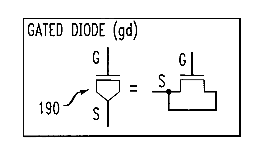
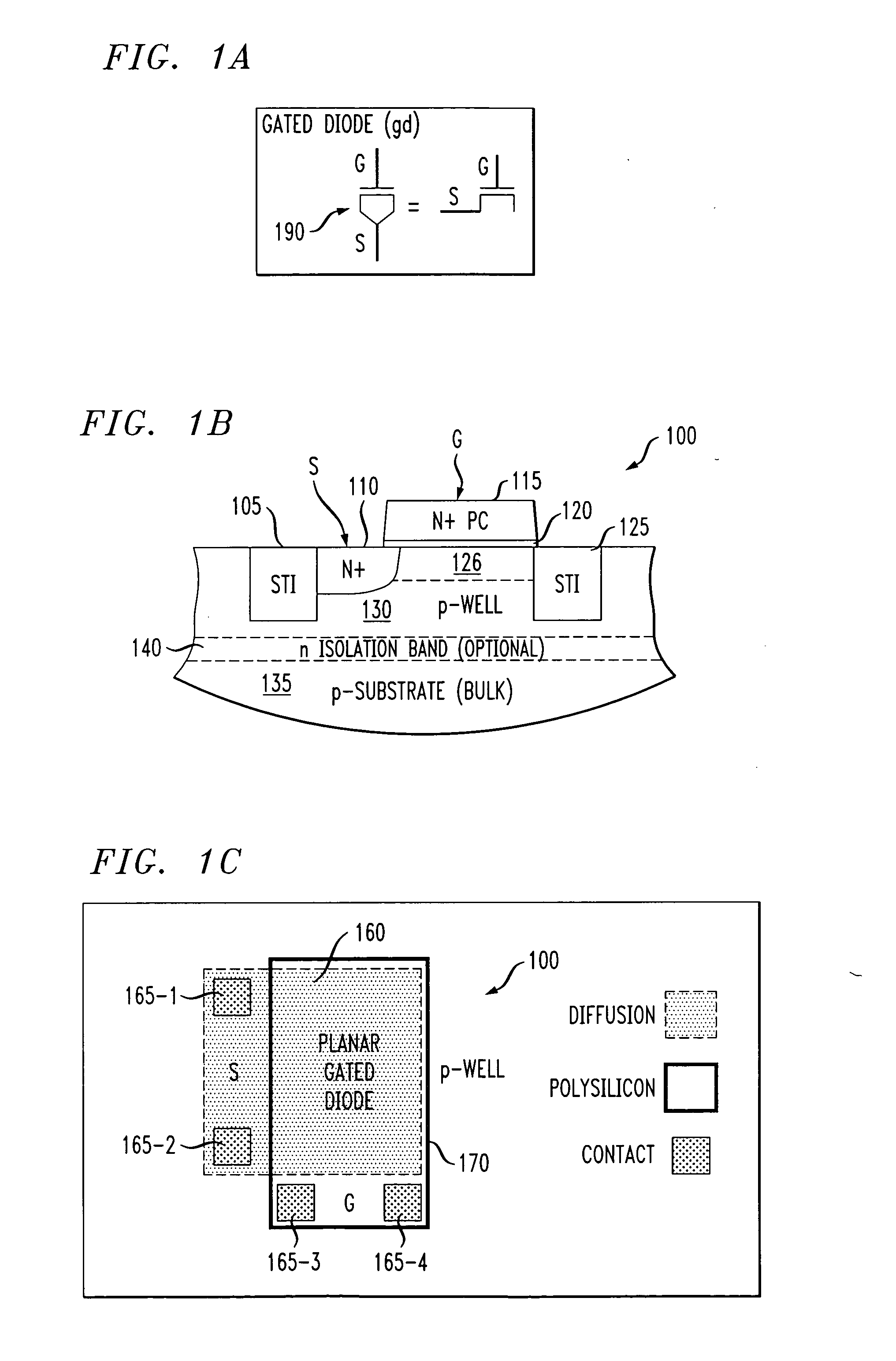
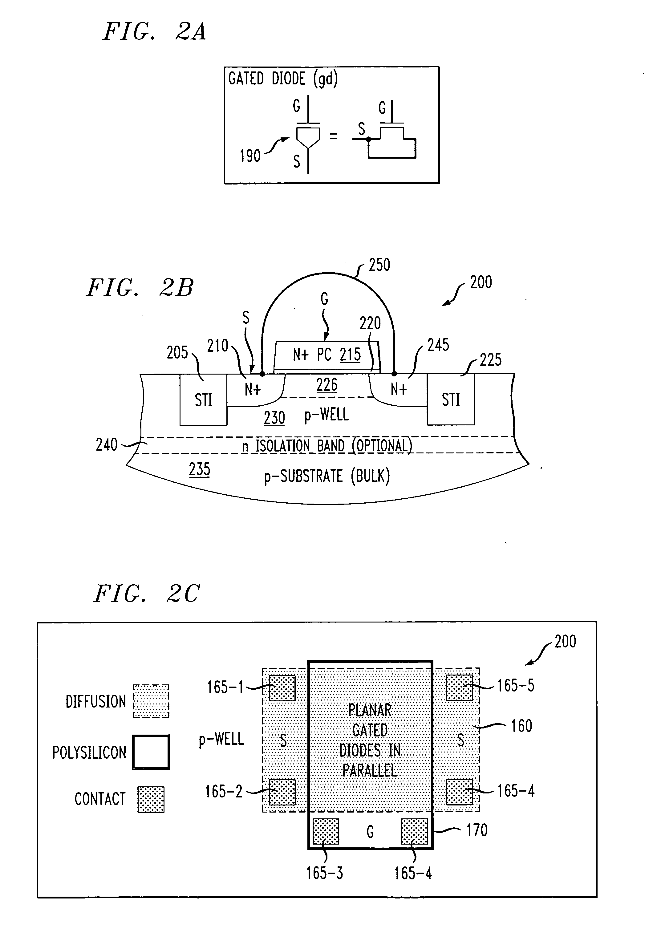
[0049] Introduction and Gated Diode Structures The term “gated diode” as used herein refers to a two terminal semiconductor device comprised of a source and a gate, where a relatively large amount of charge is stored in an inversion layer when the gate to source voltage (Vgs) is above (for an n-type gated diode) a threshold voltage, and substantially small amount, orders of magnitude smaller, or no charge is stored otherwise. As a result, the equivalent capacitance of the two terminal semiconductor device is nonlinear, meaning that the two terminal semiconductor device has a large capacitance when the voltage on the first terminal relative to the second terminal is above the threshold voltage and has a very small capacitance when the voltage on the first terminal relative to the ...


PUM


Abstract

A circuit comprises a control line and a two terminal semiconductor device having first and second terminals. The first terminal is coupled to a signal line, and the second terminal is coupled to the control line. The two terminal semiconductor device is adapted to have a capacitance when a voltage on the first terminal relative to the second terminal is above a threshold voltage and to have a smaller capacitance when a voltage on the first terminal relative to the second terminal is below the threshold voltage. The control line is coupled to a control signal and the signal line is coupled to a signal and is output of the circuit. A signal is placed on the signal line and voltage on the control line is modified (e.g., raised in the case of n-type devices, or lowered for a p-type devices). When the signal falls below the threshold voltage, the two terminal semiconductor device acts as a very small capacitor and the output of the circuit will be a small value. When the signal is above the threshold voltage, the two terminal semiconductor device acts as a large capacitor and the output of the circuit will be influenced by both the value of the signal and the value of the modified voltage on the control line and therefore the signal will be amplified.

Description

CROSS REFERENCE TO RELATED APPLICATIONS [0001] This application is related to an application by Luk et al., entitled 3T1D MEMORY CELLS USING GATED DIODES AND METHODS OF USE THEREOF, U.S. patent Ser. No. ______ filed on the same day as the present application and assigned to International Business Machines, Inc., the disclosure of which is hereby incorporated by reference.FIELD OF THE INVENTION [0002] The present invention relates to semiconductors and, more particularly, relates to semiconductor devices and circuits using the same for amplifying signals. BACKGROUND OF THE INVENTION [0003] High speed, small signal sensing amplifiers are commonly needed in memory such as Dynamic Random Access Memory (DRAM) and Static Random Access Memory (SRAM). Small signal sensing circuits are used because the current trend is toward small signal transmission over wide data buses either external or internal to a semiconductor chip. Small signal transmission is being more widely used because switchin...

Claims


Application Information

Patent Timeline
IPC IPC(8): G11C7/06H01L27/08H01L29/739H03F1/56
CPCG11C7/06H01L27/0811H03F2200/183H03F1/56H01L29/7391
Inventor LUK, WING K.DENNARD, ROBERT H.
Owner GLOBALFOUNDRIES US INC
Why Eureka
Try Eureka