Manufacturing method of solid-state image pickup device, and solid-state image pickup device

Inactive Publication Date: 2005-07-07
SHARP KK
View PDF5 Cites 10 Cited by
  • Summary
  • Abstract
  • Description
  • Claims
  • Application Information

AI Technical Summary

Benefits of technology

[0010] The present invention has been made with the aim of solving the above problems, and it is an object of the present invention to provide a manufacturing method of a solid-state image pickup device comprising a light receiving section having a photoelectric conversion region with a greater depth and less defects than a light receiving section (photoelectric conversion region) of a conventional solid-state image p

Problems solved by technology

However, when ions are implanted at an ion implantation angle that does not allow channeling, the depth of ion implantation is of course shallower compared to that obtained in conditions that allow channeling, and the implanted ions do not reach a region located at a depth of 4 μm to 6 μm from the surface of the semiconductor substrate which should essentially function as the light receiving section (photoelectric conversion region), and consequently the photoelectric conversion region is not formed.
In order to realize this ion implantation, since a large accelerator for producing the ion implantation energy is neces

Method used


Image

  • Manufacturing method of solid-state image pickup device, and solid-state image pickup device
  • Manufacturing method of solid-state image pickup device, and solid-state image pickup device
  • Manufacturing method of solid-state image pickup device, and solid-state image pickup device

Examples


Example

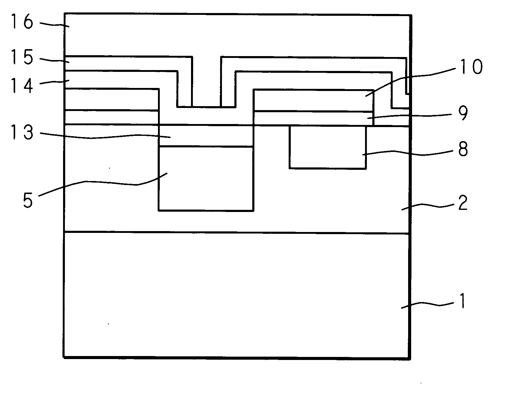
[0030] The following description will explain the present invention, based on the drawings illustrating an embodiment thereof.

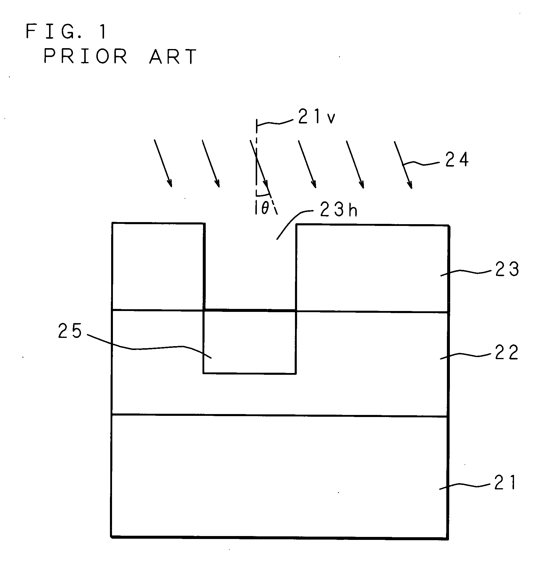
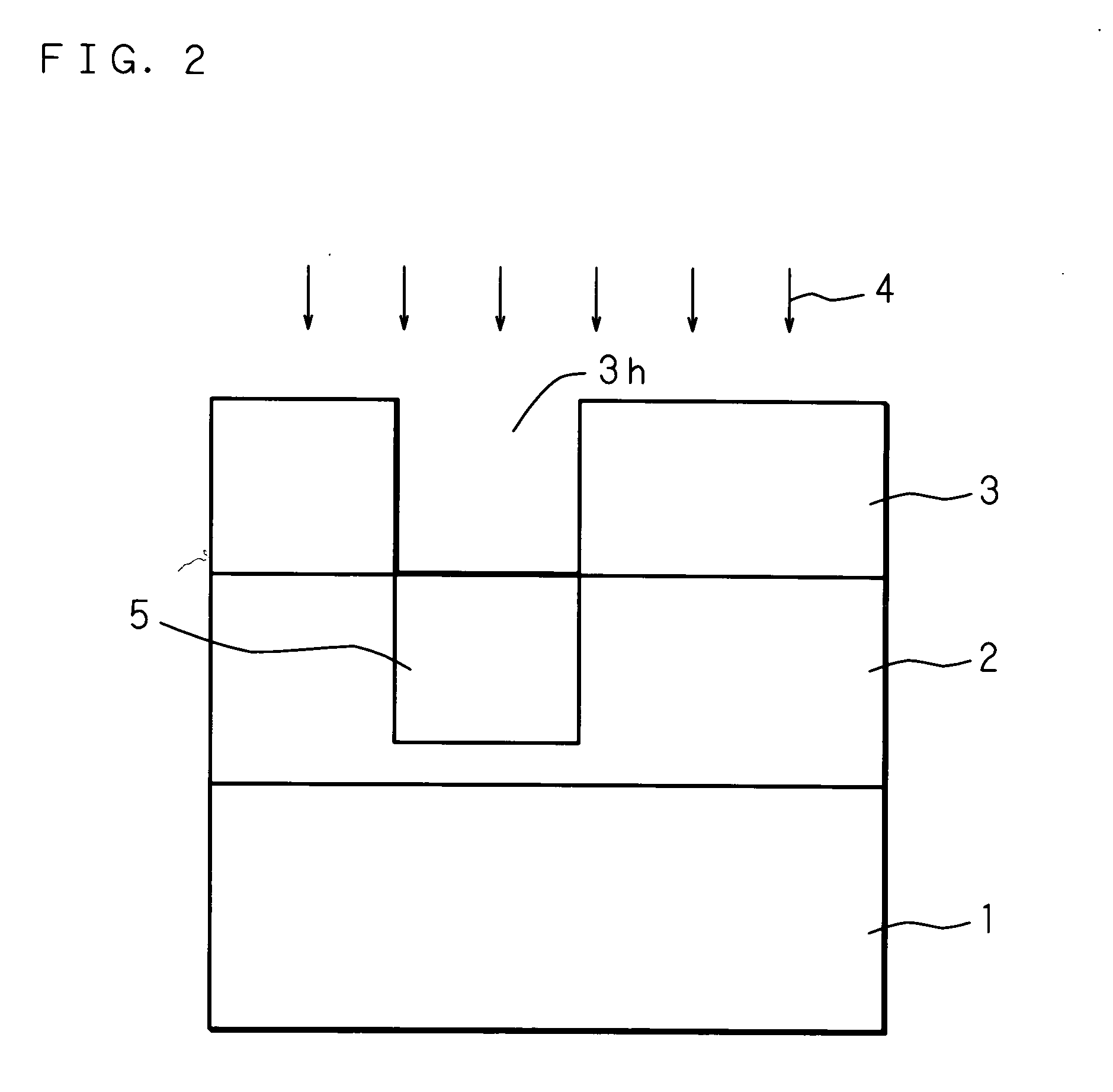
[0031]FIG. 2 through FIG. 6 are cross sectional views for explaining the state in each manufacturing step of a solid-state image pickup device according to an embodiment of the present invention. Each of the drawings shows a cross section, but oblique lines are all omitted to allow the drawings to be easily seen. FIG. 7 is a plan view for explaining a notch of a semiconductor substrate (or an orientation flat of a semiconductor substrate in a wafer state) according to an embodiment of the present invention. The notch is provided to fix a reference position of the wafer. For example, the notch has a triangular form and the top thereof is round.

[0032]FIG. 2 is a cross sectional view for explaining the state of ion implantation for forming a p-type region of a light receiving section (photoelectric conversion section). For example, a semiconductor substrate 1 ...


PUM


Abstract

A p-type region of a light receiving section is formed by implanting boron ions from the direction normal to a semiconductor substrate. The ion implantation conditions of boron are a few hundred to 4 MeV for the ion implantation energy, 1×10¹⁰ to 1×10¹² ions/cm2 for the implanted dose, and 0 degree±0.2 degrees for an ion implantation angle (θ) with respect to the direction normal to the surface of the semiconductor substrate.

Description

CROSS-REFERENCE TO RELATED APPLICATION [0001] This non-provisional application claims priority under 35 U.S.C. §119(a) on Patent Application No. 2003-431563 filed in Japan on Dec. 25. 2003, the entire contents of which are hereby incorporated by reference. BACKGROUND OF THE INVENTION [0002] The present invention relates to a method of manufacturing a solid-state image pickup device comprising a light receiving section formed by ion implantation, and also relates to a solid-state image pickup device. [0003] In a conventional manufacturing method of a solid-state image pickup device, after a transfer section and a light receiving section having a p-n junction (photoelectric conversion region) are formed by implanting ions into a semiconductor substrate, such as silicon, and a gate oxide film is formed, a gate electrode is formed by a polycrystalline material obtained by CVD (chemical vapor deposition). The light receiving section comprises a p-well formed by implanting boron ions as a...

Claims


Application Information

Patent Timeline
IPC IPC(8): H01L27/148H01L21/00H01L21/265H01L27/14H01L27/146H01L31/00H01L31/10H04N5/335H04N5/369
CPCH01L27/14689H01L27/14843Y02E10/547H01L31/1804H01L31/103Y02P70/50H01L27/146H01L31/10
Inventor SAITOH, SATOSHI
Owner SHARP KK
Why Eureka
Try Eureka