RF and MMIC stackable micro-modules

a stackable micro-module and stackable technology, applied in the direction of printed circuit manufacturing, printed circuit aspects, basic electric elements, etc., can solve the problems of significant signal attenuation, vertical integration system, etc., and achieve the effect of not being suitable for very high frequency devices or multiple modules, vertical stacking devices, and high frequency performance of the resulting

Inactive Publication Date: 2005-07-07
AGENCY FOR SCI TECH & RES
View PDF6 Cites 111 Cited by
  • Summary
  • Abstract
  • Description
  • Claims
  • Application Information

AI Technical Summary

Benefits of technology

[0007] A principal object of the present invention is to provide an effective and very manufacturable method to form vertical, integrated circuit interconnects.

Problems solved by technology

A major limitation of the above-described approaches to three-dimensional integration is the high frequency performance of the resulting, vertically integrated system.
However, when high frequency signals are carried vertically through the bulk substrate, the low resistivity proves to be lossy and results in significant signal attenuation.
However, the RF performance is still not suitable for very high frequency devices or for multiple module, vertically stacked devices.
The vertically passed signal simply interacts with the substrate too much and results in signal attenuation.
In addition, the prior art techniques used for passing signals through the substrate exhibit poor impedance matching and therefore result in lossy RF performance.
The prior art approaches have a major limitation.
These approaches cannot provide controllable dielectric thicknesses within design requirements.

Method used


Image

  • RF and MMIC stackable micro-modules
  • RF and MMIC stackable micro-modules
  • RF and MMIC stackable micro-modules

Examples


Embodiment Construction

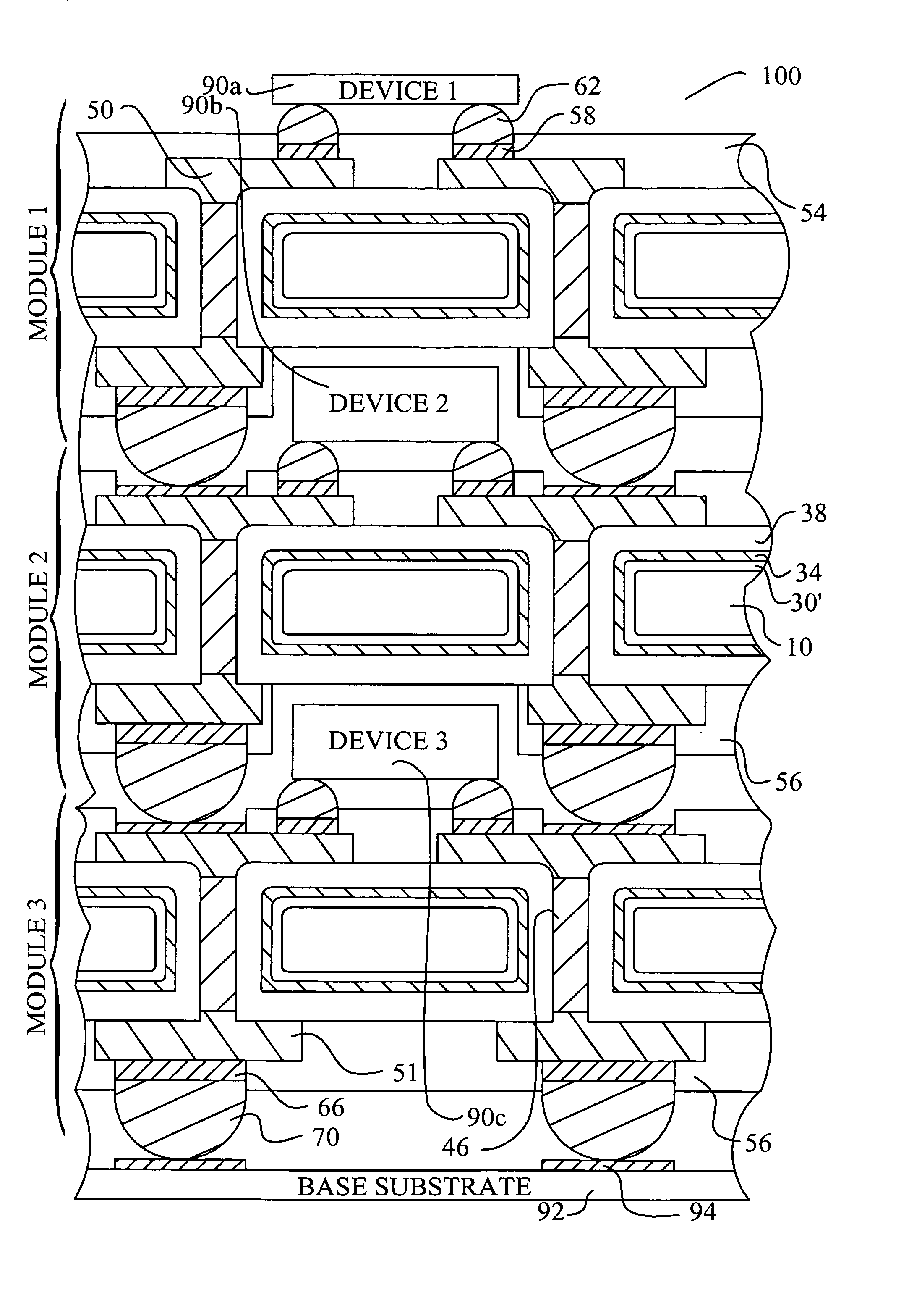
[0022] The preferred embodiments of the present invention disclose methods to form interconnection structures in the manufacture of integrated circuit devices. A method to form shielded vias with microstrip ground plane for passing signals between top and bottom sides of substrates is disclosed. A method to form a silicon carrier module for stacking integrated circuit devices is disclosed. A method to form stacked, multiple integrated circuit modules is disclosed. Interconnection and module devices are disclosed. It should be clear to those experienced in the art that the present invention can be applied and extended without deviating from the scope of the present invention.

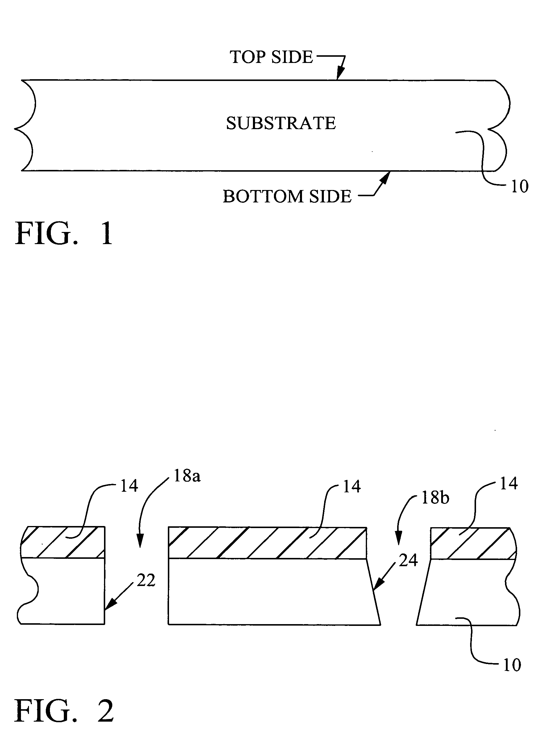
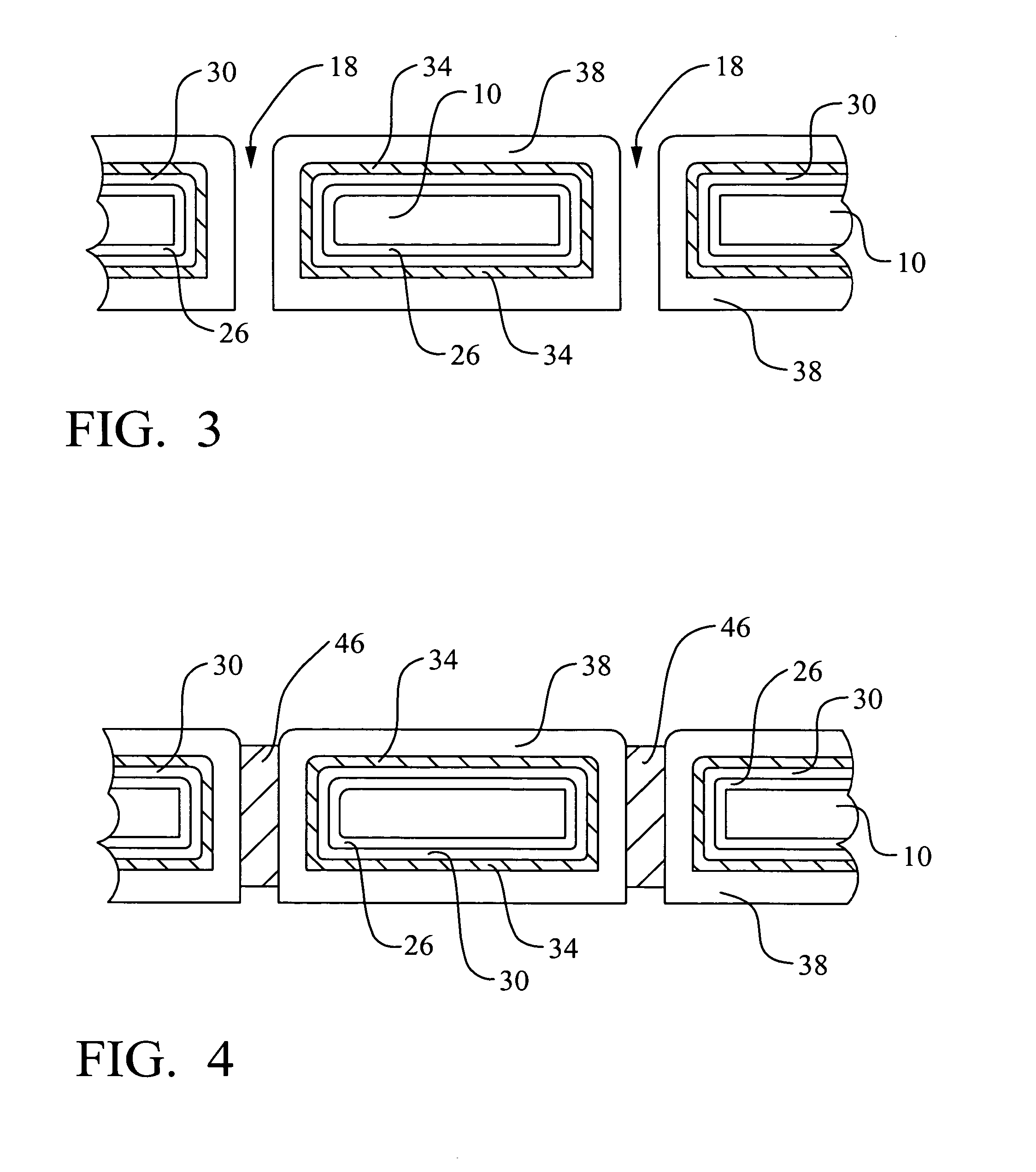
[0023] Referring now to FIGS. 1 through 9, the first preferred embodiment of the present invention is illustrated. Several important features of the present invention are shown and discussed below. The present invention provides a method to fabricate wafer-level interconnects exhibiting greatly improved RF perfo...


PUM

PropertyMeasurementUnit
resistanceaaaaaaaaaa
thicknessaaaaaaaaaa

Abstract

A new method to form shielded vias with microstrip ground plane in the manufacture of an integrated circuit device is achieved. The method comprises, first, providing a substrate. The substrate is etched through to form holes for planned shielded vias with microstrip ground plane. A first dielectric layer is formed overlying the top side of the substrate and lining the holes. A first conductive layer is deposited overlying the first dielectric layer and lining the holes. A second dielectric layer is deposited overlying the first conductive layer and lining the holes. A second conductive layer is deposited overlying the second dielectric layer and filling the holes. The second conductive layer is planarized to confine the second conductive layer to the holes and to thereby complete the shielded vias with microstrip ground plane. Silicon carrier modules and stacked, multiple integrated circuit modules are formed using shielded vias with microstrip ground plane to improve RF performance.

Description

BACKGROUND OF THE INVENTION [0001] (1) Field of the Invention [0002] The invention relates to a method to form an integrated circuit device, and, more particularly, to a method to form an interconnecting structure for use in integrating multiple, RF and MMIC stackable modules. [0003] (2) Description of the Prior Art [0004] In the art of integrated circuits, electrical interconnection and packaging are key enabling technologies. Much recent work has been done to integrate multiple devices in three dimensions. That is, many universities and research institutes are now working on technologies to reduce the volume of and to improve the performance of integrated systems of multiple ICs. In this regard, silicon stacking and through wafer interconnects have been successfully demonstrated in the art. A stacked silicon system is one where multiple integrated circuit devices are vertically stacked, one upon another. Stacking circuit modules creates area efficiencies in the same way that a hig...

Claims


Application Information

Patent Timeline
Patent Type & Authority Applications(United States)
IPC IPC(8): H01L21/48H01L21/8238H01L23/498H01L23/66H01L25/065H05K1/02H05K1/11
CPCH01L21/486Y10T29/49117H01L23/66H01L25/0657H01L25/105H01L2223/6622H01L2224/16H01L2924/01078H01L2924/01079H01L2924/15311H01L2924/3011H01L2924/3025H05K1/0222H05K1/115H05K2201/0949H05K2201/09809H01L2225/1023H01L2225/1058Y10T29/49156Y10T29/49165H01L23/49827
Inventor KRIPESH, VAIDYANATHANROTARU, MIHAI DRAGOSPERIASAMY, GANESH VETRIVELYOON, SEUNG UKNAGARAJAN, RANGANATHAN
Owner AGENCY FOR SCI TECH & RES
Why Eureka
Try Eureka