Method for forming rectangular-shaped spacers for semiconductor devices

a technology of semiconductor devices and spacers, which is applied in the field of semiconductor device spacer formation and source/drain formation, can solve the problems of reducing the conformity of subsequent film deposition, the outer shape of the spacer, and the poor so as to improve the conformity of further film deposition and the control of the source/drain implantation process

Active Publication Date: 2005-07-07
GLOBALFOUNDRIES US INC
View PDF8 Cites 9 Cited by
  • Summary
  • Abstract
  • Description
  • Claims
  • Application Information

AI Technical Summary

Benefits of technology

[0007] There is a need for a method of forming a spacer and a semiconductor device that provides for increased control of the source / drain implantation process, as well as improving conformity for further film deposition.
[0009] By providing a protective layer on the spacer layer, the sidewall of the spacer is protected during the etching process, so that a substantially rectangular (I-shaped) spacer is formed. The spacer according to the present invention therefore does not have a thinner outer edge that makes the implantation profile difficult to control. Also, the relatively vertical outer wall of the spacer increases conformity for further film deposition, such as double spacer processes or interconnect layer dielectrics.

Problems solved by technology

Another disadvantage of the D-shaped spacers 18 is the worsening of conformity for further film deposition, necessary in such processes as the formation of a double spacer or the forming of an interconnect layer dielectric.
The sloping nature of the outer shape of the spacers reduces conformity in subsequent film depositions.

Method used


Image

  • Method for forming rectangular-shaped spacers for semiconductor devices
  • Method for forming rectangular-shaped spacers for semiconductor devices
  • Method for forming rectangular-shaped spacers for semiconductor devices

Examples


Embodiment Construction

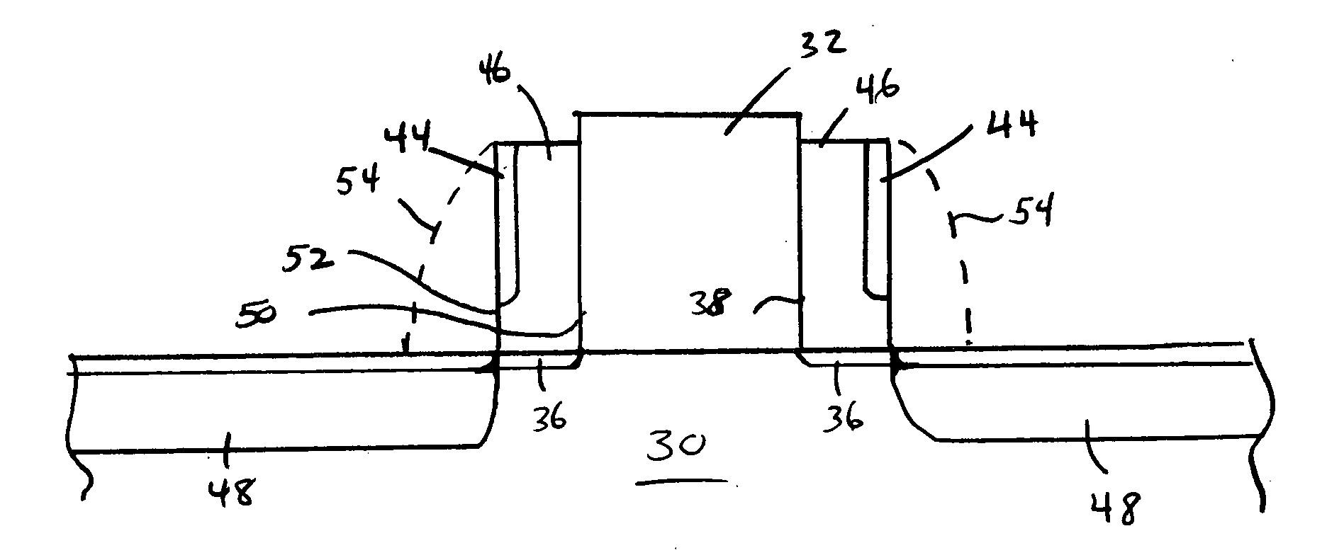
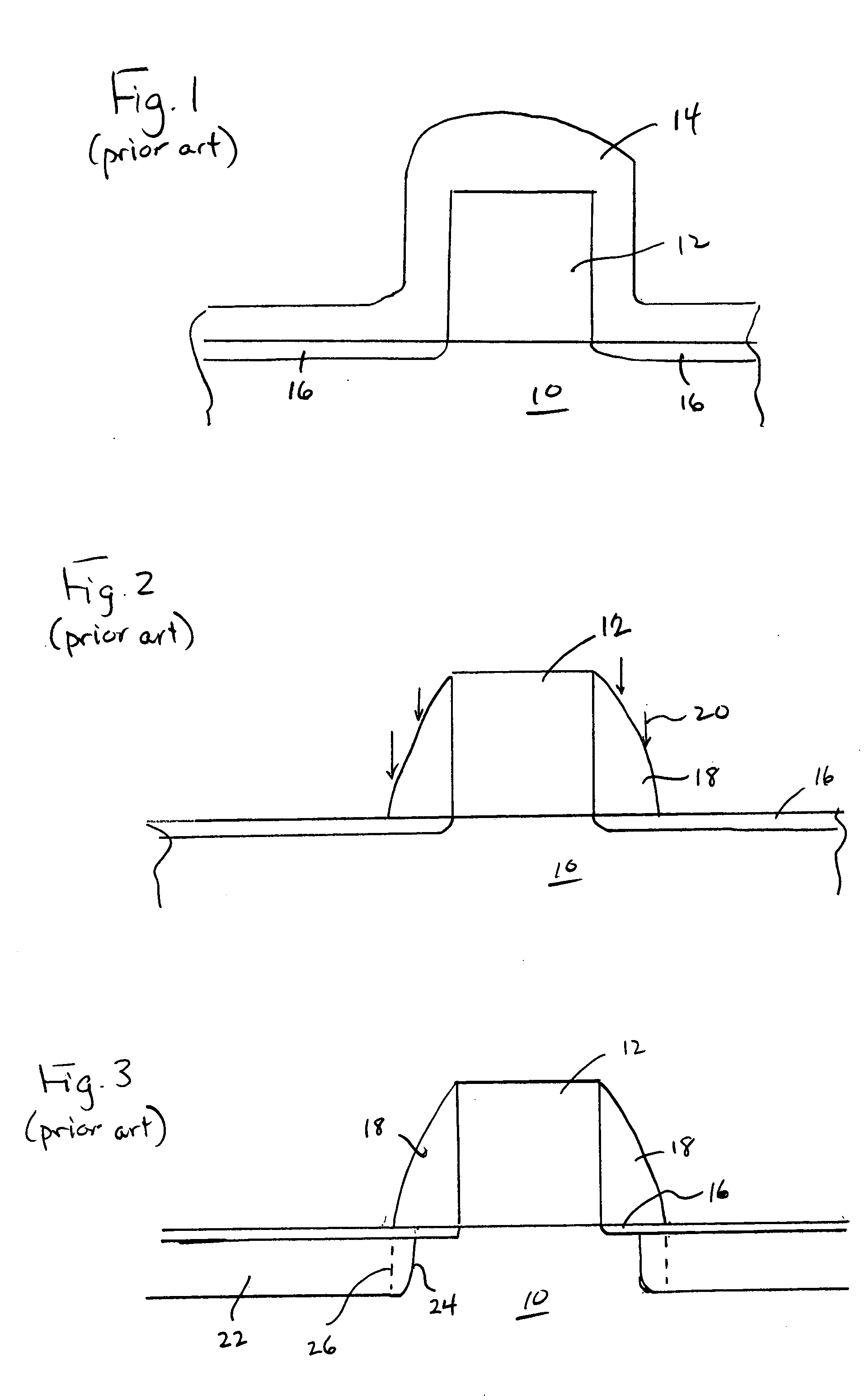
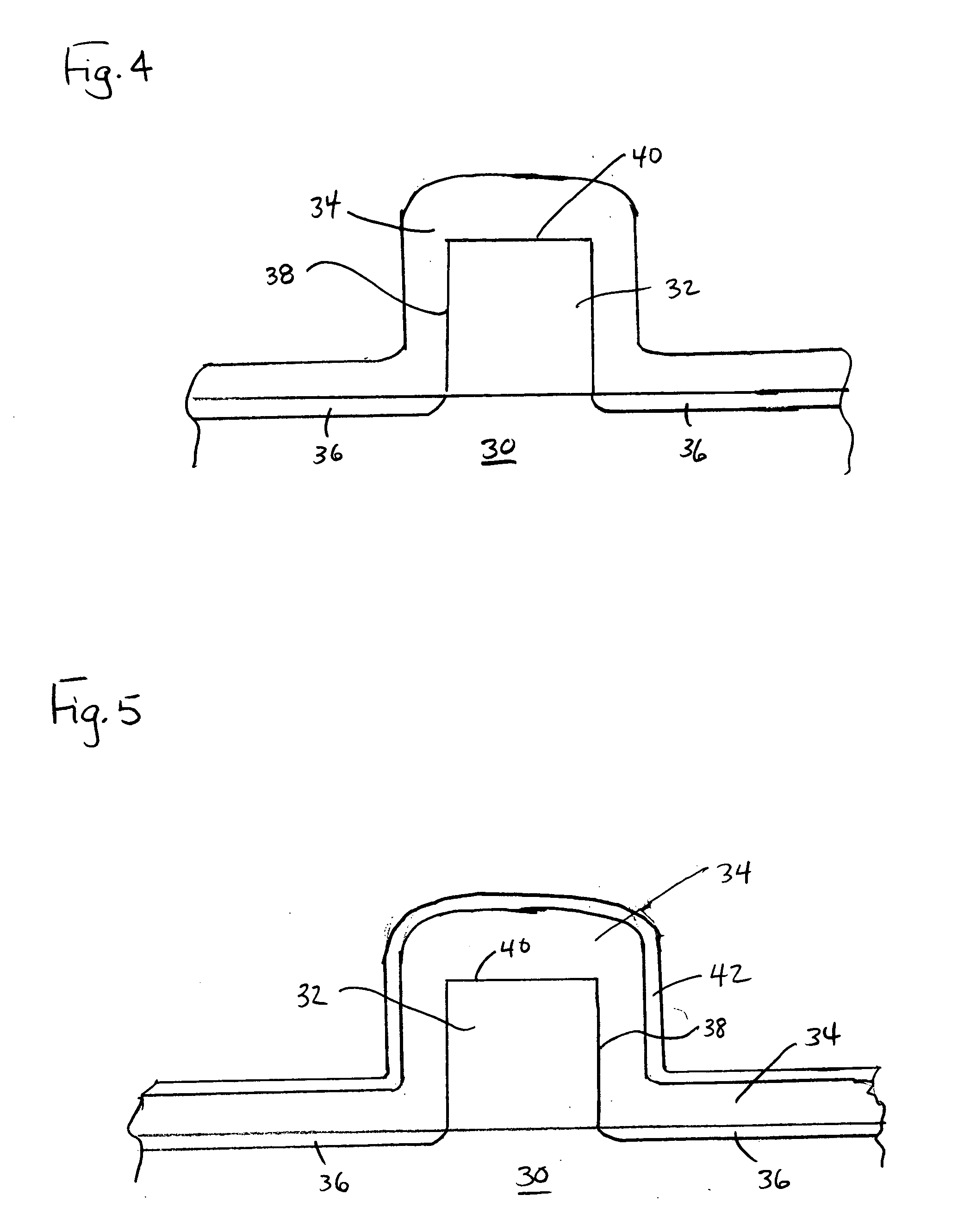
[0021] The present invention addresses and solves problems related to the formation of spacers and the source / drain implantation dose profile in advanced CMOSFET device technology. In particular, the invention overcomes problems related to the relatively thinner outer edge of the spacer created in the prior art with a D-shape that allowed punch-through during the source / drain implantation process, degrading the control of the implant dose profile. The invention achieves improvement in the implant dose profiling during the source / drain implantation process by creating a substantially rectangular (I-shape) spacer on the gate and employing the spacer as a mask during the source / drain implantation process. Since the spacer of the present invention does not have a thinner region through which punch-through may occur, the invention provides a precise source / drain implantation dose profiling. A further advantage is the increased conformity provided due to the steep sidewalls, allowing for ...


PUM


Abstract

A semiconductor device and method of making the same forms a spacer by depositing a spacer layer over a substrate and a gate electrode and forms a protective layer on the spacer layer. The protective layer is dry etched to leave a thin film sidewall on the spacer layer. The spacer layer is then etched, with the protective layer protecting the outer sidewalls of the spacer layer. This etching creates spacers on the gate that have substantially vertical sidewalls that extend parallel to the gate electrode sidewalls. The I-shape of the spacers prevent punch-through during the source / drain ion implantation process, providing an improved source / drain implant dose profile.

Description

FIELD OF THE INVENTION [0001] The present invention relates to the field of semiconductor processing, and more particularly, to the formation of spacers and source / drain formation in semiconductor devices. BACKGROUND OF THE INVENTION [0002] In the formation of semiconductor devices, it is desirable to create spacers on the sidewalls of a gate to serve as masks during source / drain implantation. An exemplary spacer formation process and implantation process is depicted in FIGS. 1-3 described below. [0003] In FIG. 1, a substrate 10 has a gate 12 formed thereon. The gate 12 may be a polysilicon gate, for example. Source / drain extension regions 16 are formed, by ion implantation, for example, employing the gate 12 as an implantation mask. A spacer layer 14 is deposited by any suitable method, such as chemical vapor deposition. The spacer layer may be made of any suitable material, such as silicon nitride, silicon oxide, low-k dielectric materials, etc. [0004] An isotropic etching is perf...

Claims


Application Information

Patent Timeline
Patent Type & Authority Applications(United States)
IPC IPC(8): H01L21/266H01L21/336
CPCH01L21/266H01L29/6659H01L29/6656H01L21/18
Inventor ZHONG, HUICAIDAKSHINA-MURTHY, SRIKANTESWARA
Owner GLOBALFOUNDRIES US INC
Why Eureka
Try Eureka