

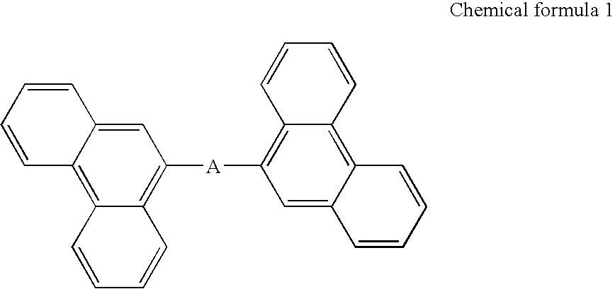
Organic electroluminescence device
- Summary
- Abstract
- Description
- Claims
- Application Information
AI Technical Summary
Benefits of technology
Problems solved by technology
Method used
Image


Examples
example 1
[0032] An ITO glass was patterned to have a luminescence area of 3 mm×3 mm, and then washed.
[0033] Then, the substrate is mounted to a vacuum chamber, the base pressure was set to 1×10⁻⁶ Torr, and then organic materials were deposited on the ITO in the order of HIL(600Å) / NPD(300Å) / CBP+1r(ppy)3(8%)(200Å) / BL-01(100Å)(hole blocking layer) / Alq3(300Å) / LiF(5Å) / Al(1000Å).
[0034] The luminescence showed 2,625 cd / m2 (8.16V) at 1 mA, where x and y are 0.286 and 0.628, respectively, on CIE chromaticity diagram.
example 2
[0035] An ITO glass was patterned to have a luminescence area of 3mm×3 mm, and then washed.
[0036] Then, the substrate is mounted to a vacuum chamber, the base pressure was set to 1×10⁻⁶ Torr, and then organic materials were deposited on the ITO in the order of HIL(600Å) / NPD(300Å) / CBP+1r(ppy)3(8%)(200Å) / BL-25(100Å)(hole blocking layer) / Alq3(300Å) / LiF(5Å) / Al(1000Å).
[0037] The luminescence showed 3,209 cd / m2 (8.18V) at 1 mA, where x and y are 0.287 and 0.627, respectively, on CIE chromaticity diagram.
PUM
| Property | Measurement | Unit |
|---|---|---|
| Luminescence | aaaaa | aaaaa |
Abstract
Description
Claims
Application Information