High performance strained CMOS devices

a technology of cmos and high-performance, applied in the field of semiconductor devices, can solve the problems of p-fets, deterioration of electron mobility, and significant increase in hole mobility

Inactive Publication Date: 2005-07-07
GLOBALFOUNDRIES INC
View PDF40 Cites 130 Cited by
  • Summary
  • Abstract
  • Description
  • Claims
  • Application Information

AI Technical Summary

Benefits of technology

[0011] In a further aspect of the invention, a process of forming a semiconductor structure is provided. The process entails forming a first shallow trench isolation. The shallow trench isolation has at least one overhang configured to prevent oxidation induced stress in a first determined direction. In the process, a structure is formed comprising a silicon layer, a silicon dioxide layer on the silicon layer, and a silicon nitride layer on the silicon dioxide layer. A portion of the silicon nitride layer, the silicon dioxide layer and the silicon substrate is etched to form a trench. Sidewall portions of the silicon nitride layer in the trench are etched to create a recession of the silicon nitride layer relative to the trench. A shallow trench isolation is formed in the trench, which in embodiments has an overhang.

Problems solved by technology

This is significant because such strain affects performance (e.g., electron and hole mobility).
While strain may improve electron mobility in n-channel field effect transistors (nFETs), performance improvement (i.e., enhancement of hole mobility) in p-channel field effect transistors (p-FETs) poses a greater challenge.
Compressive stress applied in the longitudinal direction with respect to the current flow may cause a significant increase in hole mobility, but may also degrade electron mobility.
This stress can substantially affect performance, such as adversely by decreasing nFET electron mobility.
In particular, Si located adjacent to the vertical portion of an STI is susceptible to oxidation induced stress.
The increased thickness induces stress in the silicon active area, which can affect performance, such as adversely by decreasing nFET electron mobility.
As efforts to miniaturize and incorporate more active devices on a single substrate continue, it becomes increasingly likely that such sources of stress will be close enough to appreciably impact performance.

Method used


Image

  • High performance strained CMOS devices
  • High performance strained CMOS devices
  • High performance strained CMOS devices

Examples


Embodiment Construction

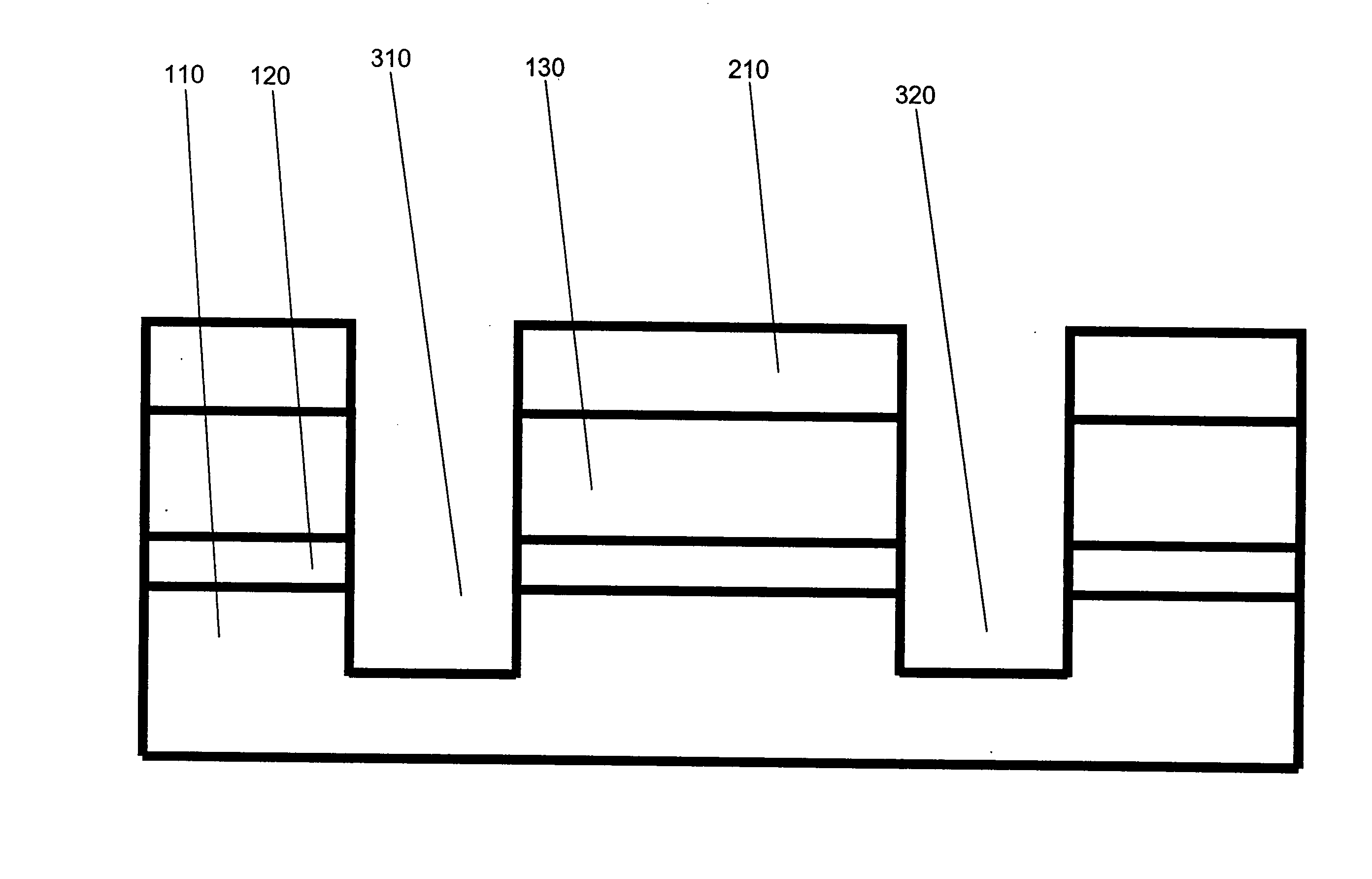
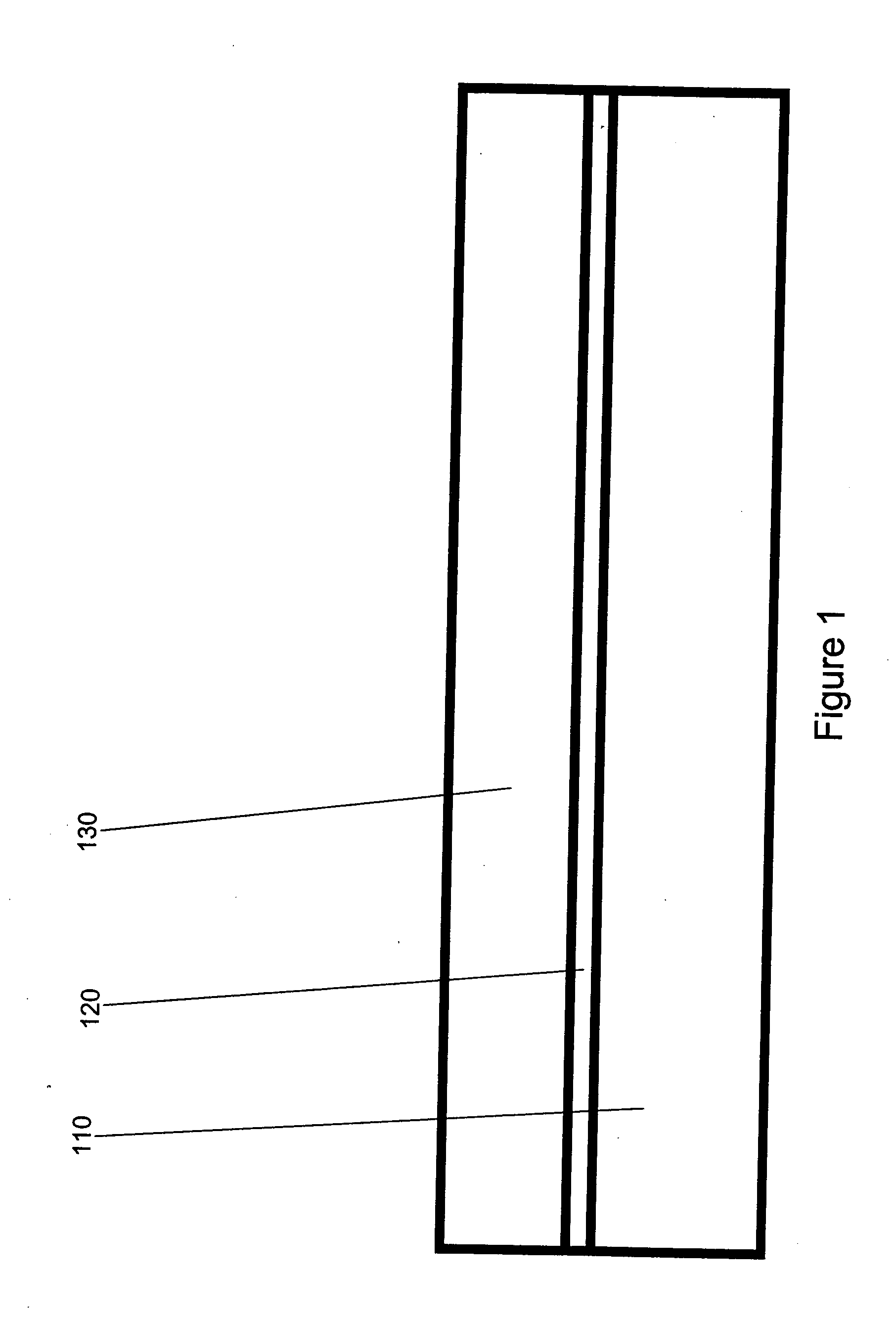
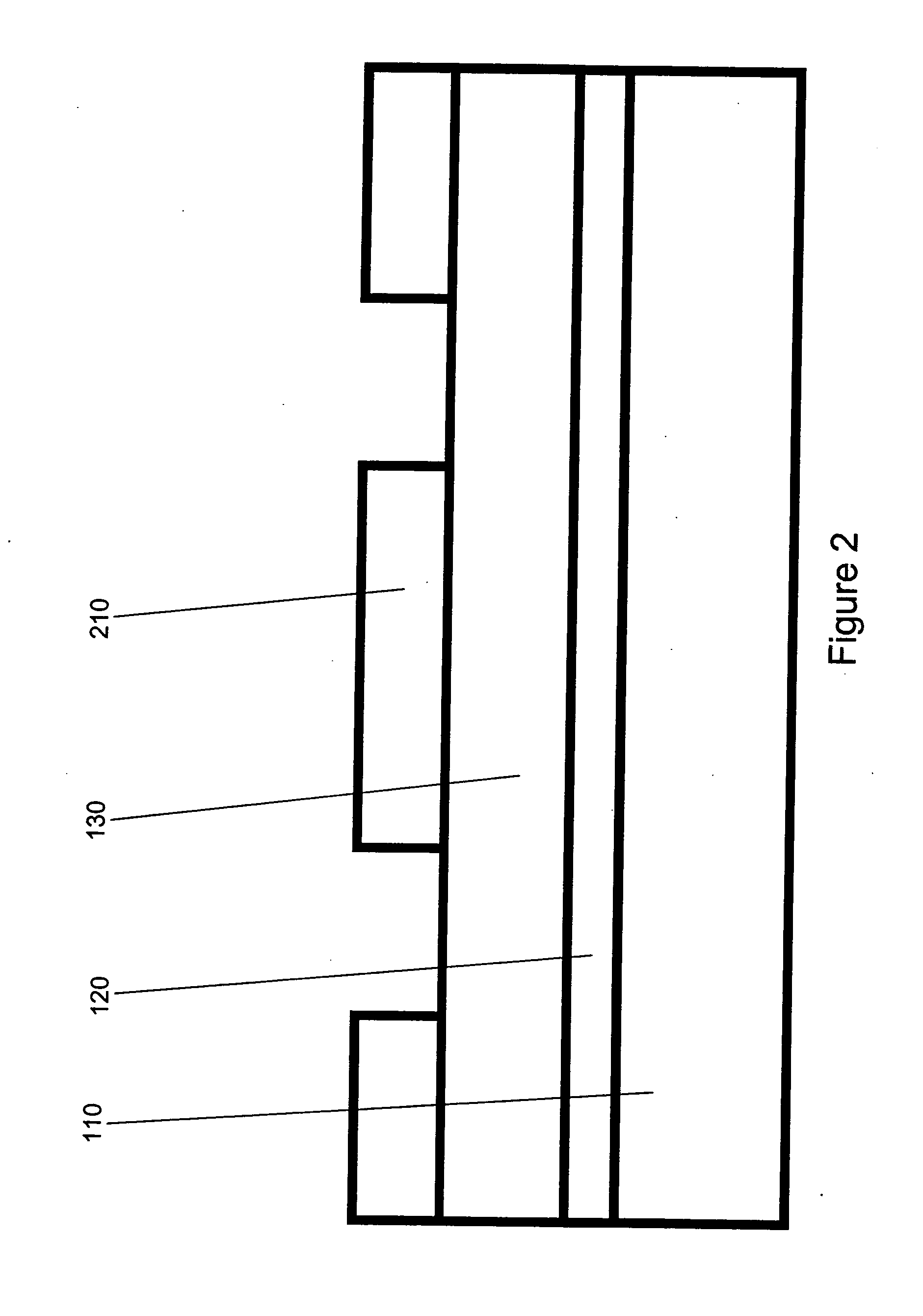
[0023] The invention employs a silicon nitride (Si3N4) pull-back process in combination with a mask used to prevent the Si3N4 pull-back from being executed in the longitudinal components of some or all pFET devices. The resulting semiconductor structure has overhang structures (referred to herein as overhang, SiO2 overhang, and STI overhang) present for nFET devices in the directions of and transverse to current flow. To enhance performance due to compressive stresses, no silicon dioxide (SiO2) overhang is present in the direction parallel to the direction of current flow for pFET devices.

[0024] However, the structure has SiO2 overhangs in the direction transverse to current flow for pFET devices to avoid performance degradation from compressive stresses. The overhang structures prevent oxidation by blocking access to underlying Si. Without an overhang, Si at the vertical Si—SiO2 interface adjacent to the shallow trench isolation would be susceptible to oxidation and attendant volu...


PUM


Abstract

A semiconductor device and method of manufacture provide an n-channel field effect transistor (nFET) having a shallow trench isolation with overhangs that overhang Si—SiO2 interfaces in a direction parallel to the direction of current flow and in a direction transverse to current flow. The device and method also provide a p-channel field effect transistor (pFET) having a shallow trench isolation with an overhang that overhangs Si—SiO2 interfaces in a direction transverse to current flow. However, the shallow trench isolation for the pFET is devoid of overhangs, in the direction parallel to the direction of current flow.

Description

BACKGROUND OF THE INVENTION [0001] 1. Field of the Invention [0002] The invention generally relates to a semiconductor device and method of manufacture and, more particularly, to a complementary metal-oxide-semiconductor (CMOS) device that includes shallow trench isolations (STI) overhanging interfaces thus preventing oxidation induced compressive stresses in the device. [0003] 2. Background Description [0004] CMOS devices may be fabricated using various process techniques. One method entails fabricating strained Silicon (Si) layers on relaxed Silicon Germanium (SiGe) layers. As the Germanium (Ge) concentration increases, strain in the Si lattice increases. This is significant because such strain affects performance (e.g., electron and hole mobility). While strain may improve electron mobility in n-channel field effect transistors (nFETs), performance improvement (i.e., enhancement of hole mobility) in p-channel field effect transistors (p-FETs) poses a greater challenge. Hole mobil...

Claims


Application Information

Patent Timeline
Patent Type & Authority Applications(United States)
IPC IPC(8): H01LH01L21/336H01L21/76H01L21/8238H01L29/78
CPCH01L21/823807H01L21/823878H01L29/7846H01L29/66575H01L29/78H01L21/84H01L21/76
Inventor DORIS, BRUCE D.GLUSCHENKOV, OLEG G.
Owner GLOBALFOUNDRIES INC
Why Eureka
Try Eureka