Semiconductor manufacturing system, work manufacturing system, and conveyance system

a manufacturing system and semiconductor technology, applied in the field of semiconductor device manufacturing, can solve the problems of deteriorating investment efficiency, lowering the overall utilization rate of manufacturing apparatuses, and stagnating semiconductor manufacturing, so as to improve the productivity of semiconductor devices, improve the utilization rate of each of manufacturing apparatuses in the flow shop section, and improve the production efficiency of semiconductor manufacturing steps.

Inactive Publication Date: 2005-07-07
TRECENTI TECHNOLOGIES INC
View PDF3 Cites 8 Cited by
  • Summary
  • Abstract
  • Description
  • Claims
  • Application Information

AI Technical Summary

Benefits of technology

[0035] (1) Since a utilization rate of each of the manufacturing apparatuses in a flow shop section can be improved, production efficiency in the semiconductor manufacturing steps can be significantly improved.
[0036] (2) By controlling each cell in the quasi flow shop as an independent manufact

Problems solved by technology

However, the present inventors have found out that the above-described techniques for manufacturing semiconductor devices have the following problems.
This may cause stagnation in the semiconductor manufacture.
Therefore, overall utilization of the manufactu

Method used


Image

  • Semiconductor manufacturing system, work manufacturing system, and conveyance system
  • Semiconductor manufacturing system, work manufacturing system, and conveyance system
  • Semiconductor manufacturing system, work manufacturing system, and conveyance system

Examples


first embodiment

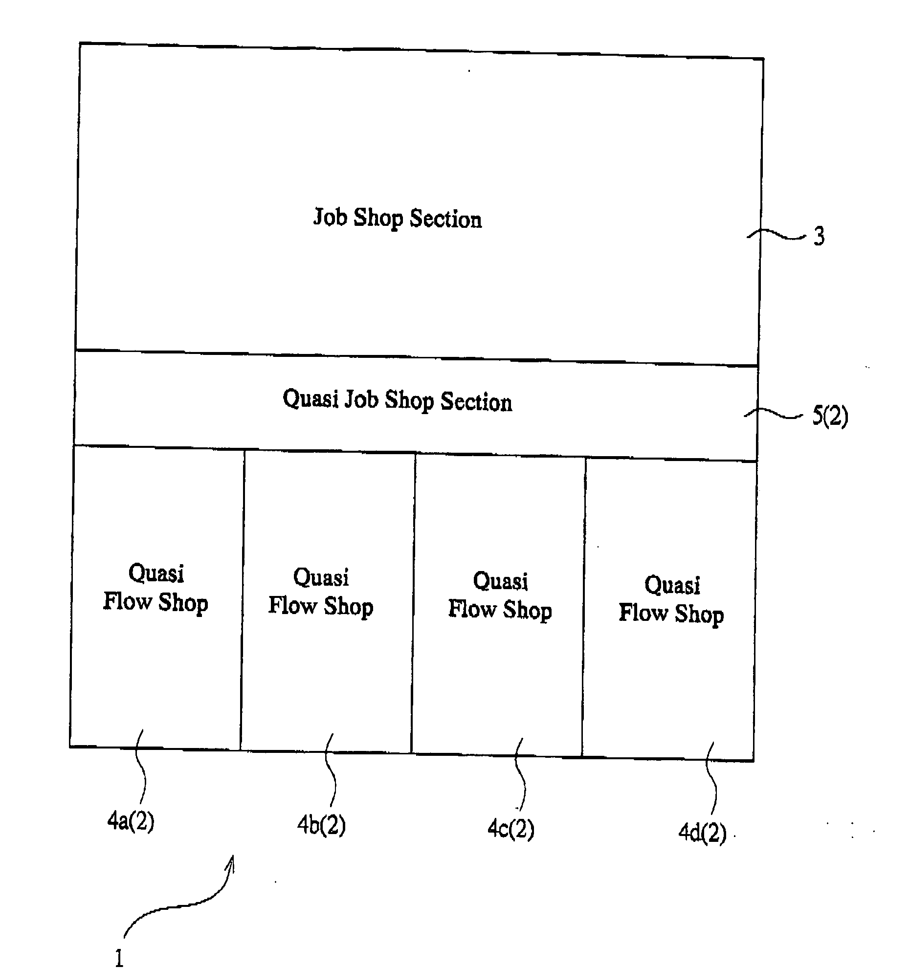
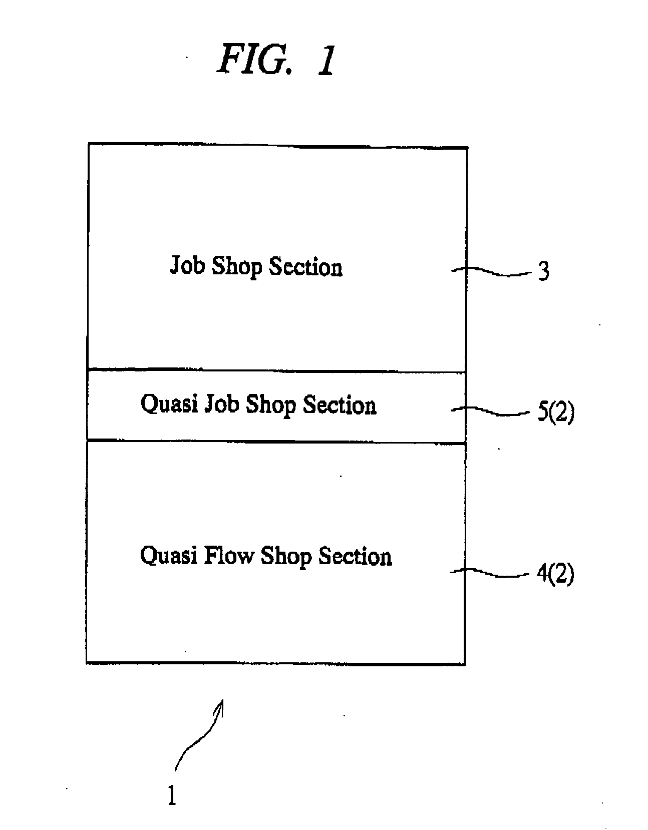
[0061] In a present first embodiment, a semiconductor manufacturing system 1 in a clean room comprises, for example, manufacturing apparatuses used in a transistor formation process etc. As shown in FIG. 1, the semiconductor manufacturing system 1 comprises a combination of a flow shop section 2 and a job shop section 3, wherein the flow shop section 2 is disposed on a lower side of FIG. 1 and the job shop section 3 is disposed on the top of the flow shop section 2.

[0062] The flow shop section 2 is an area in which the manufacturing apparatuses are sequentially disposed so as to correspond to process flow of manufacturing steps. In the section, manufacturing apparatuses used in a frequently repeated manufacturing step such as an ion implantation step and / or a wiring step (a Cu (copper) damascene step and an Al (aluminum) wiring step) are disposed.

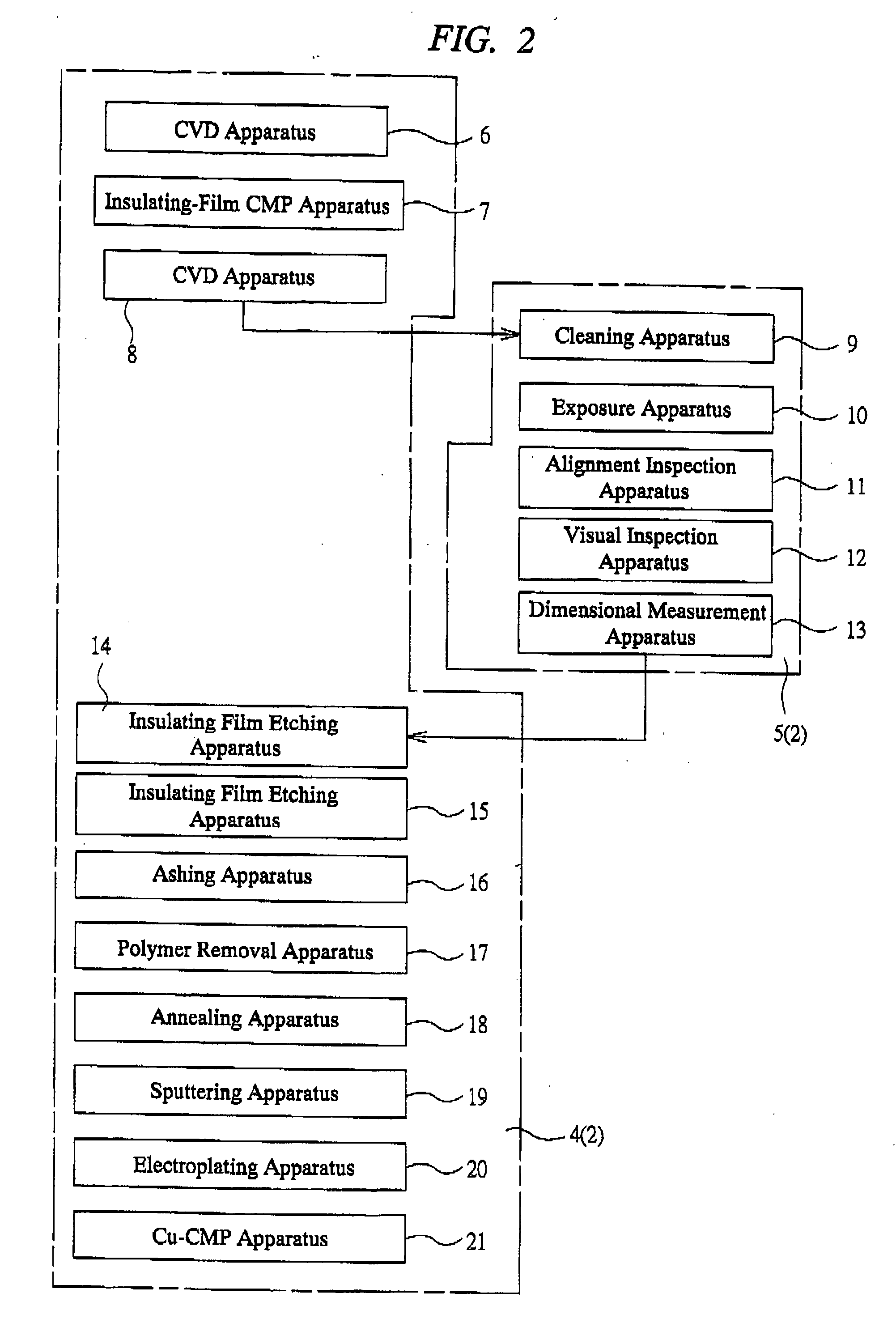
[0063] In the job shop section 3, apparatuses such as a cleaning apparatus, an oxidation apparatus, a diffusion apparatus, an LPCVD appa...

second embodiment

[0110] In a present second embodiment, a semiconductor manufacturing system 22 is a control system for semiconductor manufacture in a flow shop line, in which manufacturing apparatuses and a transfer system are consecutively disposed in order of processing steps. For example, the manufacturing apparatuses used for such as an ion implantation step and a wiring step (a Cu (copper) damascene step and an Al (aluminum) wiring step), which include a number of frequently repeated manufacturing steps, are disposed therein.

[0111] As shown in FIG. 9, a host computer 23 is provided in the semiconductor manufacturing system 22. A flow shop line is composed of a quasi flow shop 24 and a quasi job shop 25.

[0112] In the quasi flow shop 24, the manufacturing apparatuses are disposed respectively so that factors such as a processing ability difference, a maintenance frequency difference, a maintenance time difference, a failure frequency difference, and a repair time difference among the respectiv...

third embodiment

[0173] A transfer system (or conveyance system) of a present third embodiment has such a configuration that a transfer time in a direction extending along the process flow in a cell area employing a flow shop system layout becomes the shortest one.

[0174] As shown in FIG. 14, a transfer system of the present embodiment 1s configured to have a flow shop area 42 in which a plurality of manufacturing apparatuses are arranged along the flow of processes, and a guided vehicle 49 for conveying products between the plurality of manufacturing apparatuses in the flow shop area 42.

[0175] The flow shop area 42 is divided into a plurality of cell areas 43, each of which is composed of a group of manufacturing apparatuses as a minimum unit required in the step, and, in each of the cell areas 43, a plurality of manufacturing apparatuses 44 are arranged along the flow of process in a direction extending from upstream to downstream.

[0176] The guided vehicle 49 has driving wheels 51 set on a rear-...


PUM


Abstract

A semiconductor manufacturing system in a clean room is composed of a combination of a flow shop section and a job shop section. The flow shop section is composed of a quasi flow shop section and a quasi job shop section. In the quasi flow shop section, manufacturing apparatuses are arranged respectively so that a difference between processing ability of the manufacturing apparatuses is taken into consideration and a balance in productivity is achieved. In the quasi job shop section, manufacturing apparatuses are arranged respectively so that the balance in productivity is not achieved due to low or high processing ability of the manufacturing apparatuses, and are provided so as to be shared by the quasi flow shop section. Accordingly, a difference between the processing ability of the manufacturing apparatuses can be reduced and the cycle time can be significantly reduced.

Description

CROSS-REFERENCE TO RELATED APPLICATION [0001] The present application claims priority from Japanese patent application No. JP 2004-001814 filed on Jan. 7, 2004 and Nos. JP 2004-003269 and JP 2004-002851 filed on Jan. 8, 2004, the contents of which are hereby incorporated by reference into this application. BACKGROUND OF THE INVENTION [0002] The present invention relates to a technique for manufacturing a semiconductor device, and particularly to a technique effectively applied to improvement of a cycle time in semiconductor device manufacture, improvement in productivity of the semiconductor device manufacture, and transfer of employing a flow shop system layout in a transfer system which improves logistics in a flow shop layout in which a plurality of manufacturing apparatuses (or tools or a plurality of pieces of equipment) are disposed (or laid out or arranged) along flow of a process. [0003] A manufacturing technique in a manufacturing process of the semiconductor device include...

Claims


Application Information

Patent Timeline
IPC IPC(8): H01L21/02G06F19/00G06Q10/00H01L21/00H01L21/677H01L21/68
CPCG06Q10/06H01L21/67727H01L21/67276H01L21/02H01L21/68
Inventor OKADA, YOSHIOWAKABAYASHI, TAKAYUKIKOIKE, ATSUYOSHITAKEHARA, NAOKI
Owner TRECENTI TECHNOLOGIES INC
Why Eureka
Try Eureka