
Tunable semiconductor diodes

a semiconductor diode, tunable technology, applied in the direction of diodes, semiconductor devices, semiconductor/solid-state device details, etc., can solve the problems of large esd structures, increased capacitance per unit area, and inacceptable high-speed rf (radio frequency) applications, so as to reduce esd robustness and reduce capacitance

Active Publication Date: 2005-07-14
TAIWAN SEMICON MFG CO LTD
View PDF4 Cites 22 Cited by
  • Summary
  • Abstract
  • Description
  • Claims
  • Application Information

AI Technical Summary

Benefits of technology

[0010] The present invention also provides an ESD (electrostatic discharges) diode that has reduced capacitance without reduced ESD robustness.

Problems solved by technology

In a CMOS technology, this also leads to an increase in the capacitance per unit area which is acceptable for CMOS technologies below 1 GHz application frequencies but not for application speeds above this frequency range.
Large ESD structures are also unacceptable for high speed RF (Radio Frequency) applications due to the high capacitance load placed on the RF circuit.

Method used


Image

  • Tunable semiconductor diodes
  • Tunable semiconductor diodes
  • Tunable semiconductor diodes

Examples


Embodiment Construction

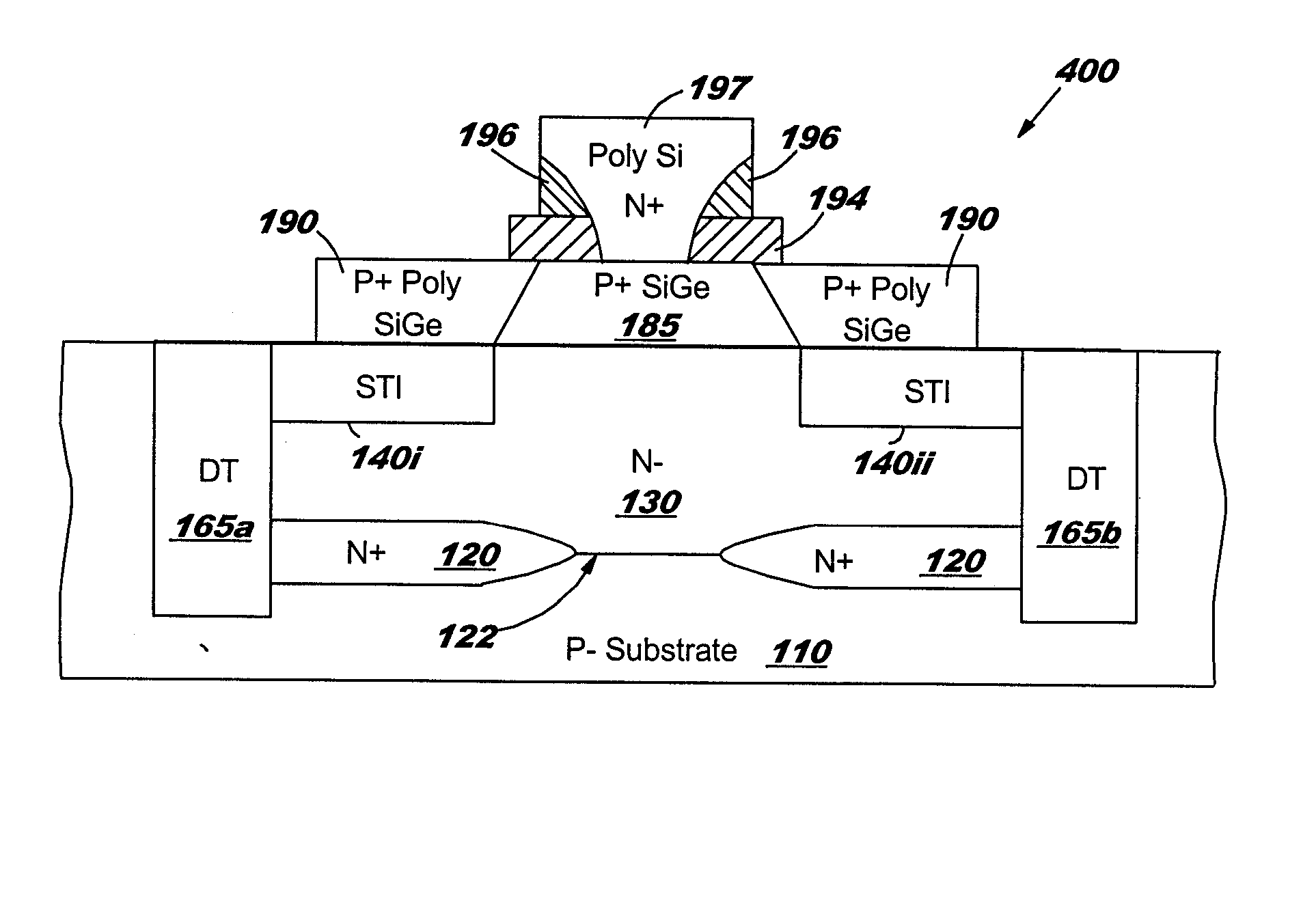
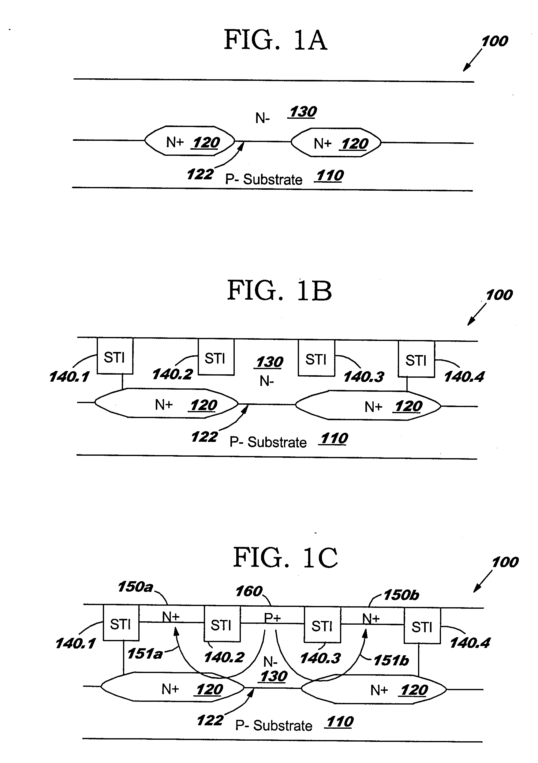
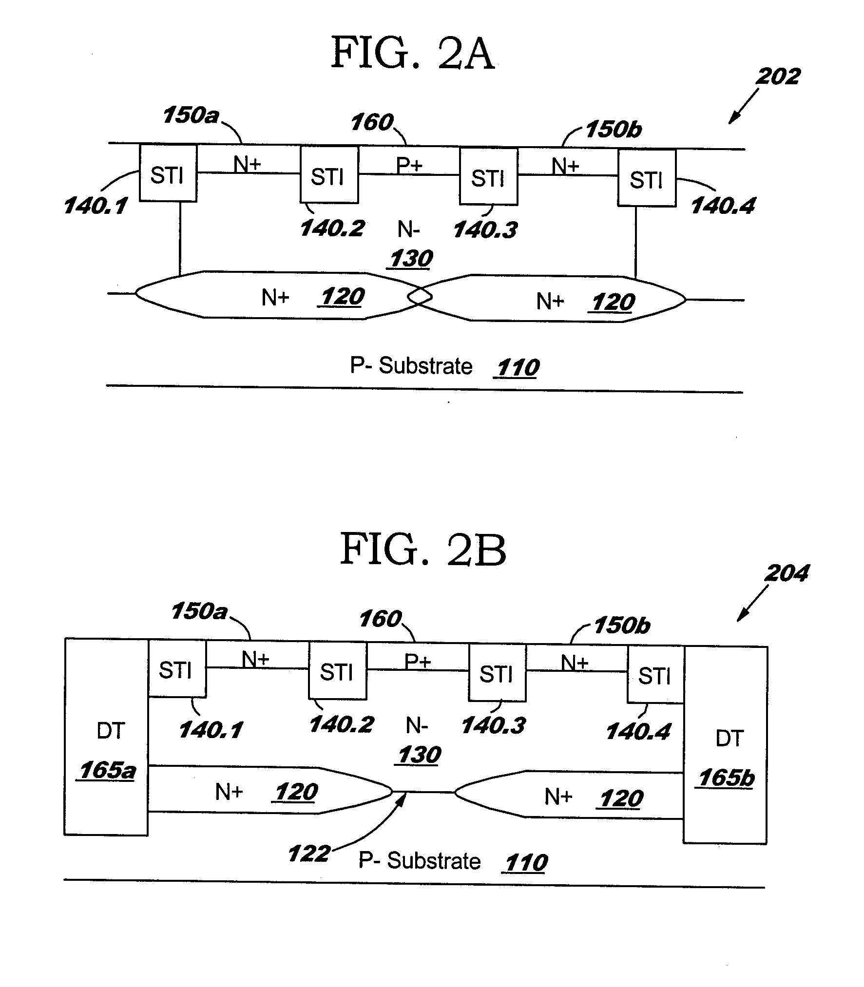
[0016] Diodes with different breakdown voltages and different capacitance loading are used in ICs (Integrated Circuits) for a variety of purposes. Diodes are used as analog circuit elements, varactors, and electrostatic discharge (ESD) circuit applications. Breakdown voltage values and loading capacitance are a concern for circuits on input pads. One purpose of using diodes is for usage as electrostatic discharge circuitry. ESD devices are used on input pins and between power rails to discharge current to the power rails, or between power rails. ESD may occur when isolated circuits with different functions coexist on the same IC. Electrostatic charge may accumulate on these isolated circuits, and needs to be discharged. Diodes can be used to connect these isolated circuits. For instance, a diode can be used to connect an electric node A belonging to a first circuit of the IC to another electric node B belonging to a second circuit of the same IC. When electrostatic charge is accumul...


PUM


Abstract

A diode structure that facilitates tuning the breakdown voltage of the diode structure, and a method for forming and operating the diode structure. In a P− substrate, a N+ layer is implanted. The N+ layer has an opening whose size affects the breakdown voltage of the diode structure. Upon the N+ layer, an N− layer is implanted in the substrate. Then, a P+ region is formed to serve as an anode of the diode structure. An N+ region can be formed on the surface of the substrate to serve as a cathode of the diode structure. By changing the size of the opening in the N+ layer during fabrication, the breakdown voltage of the diode structure can be changed (tuned) to a desired value.

Description

BACKGROUND OF INVENTION [0001] 1. Technical Field [0002] The present invention relates to semiconductor diodes, and more particularly, to tunable semiconductor diodes. [0003] 2. Related Art [0004] ESD (electrostatic discharges) diodes are well known in present day semiconductor technology in order to protect I / O and other internal circuitry from electrostatic discharges and other overvoltage conditions that could cause catastrophic failure in integrated circuits. See e.g. U.S. Pat. No. 5,629,544 to Voldman et al., “Semiconductor Diode with Silicide Films and Trench Isolation,” which teaches ESD diodes having silicided electrodes to reduce series resistance, and U.S. Pat. No. 5,945,713 to Voldman, “Electrostatic Discharge Protection Circuits for Mixed Voltage Interface and Multi-Rail Disconnected Power Grid Applications,” which teaches an ESD diode that can interface with multiple supply voltages. [0005] Because of high sheet resistance, these ESD diodes must be made large in order t...

Claims


Application Information

Patent Timeline
IPC IPC(8): H01L21/329H01L27/02H01L29/861
CPCH01L27/0255H01L29/66136H01L29/8611H01L29/8618H01L2924/0002H01L2924/00
Inventor VOLDMAN, STEVEN H.
Owner TAIWAN SEMICON MFG CO LTD
Learn More