Broadband pulse width modulation circuit and optical amplifier using the same

a technology of broadband pulse width and modulation circuit, which is applied in the direction of lasers, electromagnetic transmission, transmission, etc., can solve the problems of not solving the subject just described, the satisfaction of the requirement for a high speed response is not easy, and the signal frequency band is limited by the time constant, so as to achieve high speed responsibility, reduce power consumption, and improve power efficiency

Active Publication Date: 2005-07-14
FUJITSU LTD
View PDF2 Cites 14 Cited by
  • Summary
  • Abstract
  • Description
  • Claims
  • Application Information

AI Technical Summary

Benefits of technology

[0010] It is an object of the present invention to provide a broadband pulse width modulation circuit and an optical amplifier incorporating the same which have a desired signal band characteristic and can achieve high speed re...

Problems solved by technology

Therefore, there is a defect that a signal frequency band is limited by the time constant of the LC elements.
However, where a PWM circuit which requires a smoothing circuit having LC elements in this manner is used, since a signal frequency band i...

Method used


Image

  • Broadband pulse width modulation circuit and optical amplifier using the same
  • Broadband pulse width modulation circuit and optical amplifier using the same
  • Broadband pulse width modulation circuit and optical amplifier using the same

Examples


Embodiment Construction

[0030] [A] Description of an Embodiment

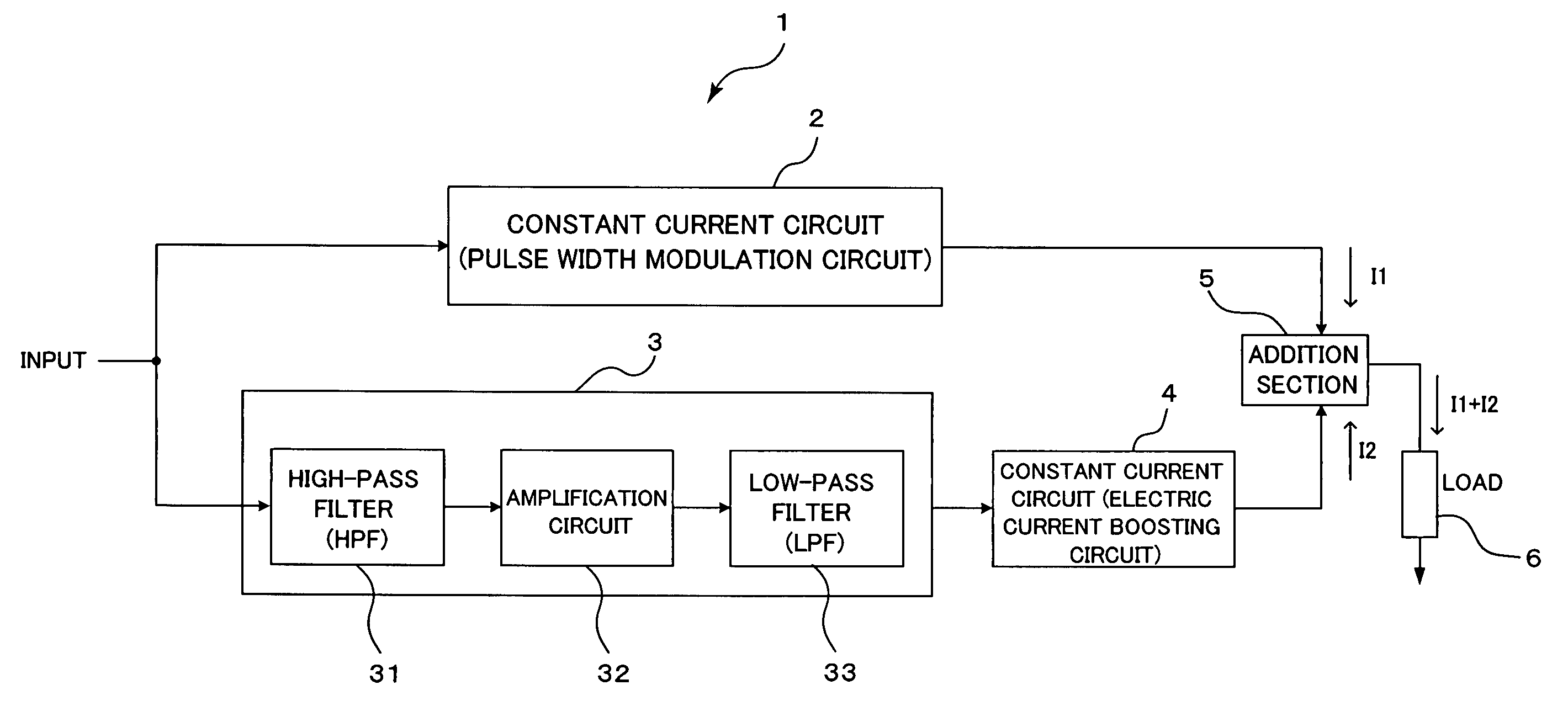
[0031]FIG. 1 is a block diagram showing a configuration of a broadband pulse width modulation (PWM) circuit as an embodiment of the present invention. The broadband PWM circuit 1 shown in FIG. 1 includes a pulse width modulation (PWM) circuit (constant current circuit) 2, a frequency band selection and amplification circuit 3, an electric current boosting circuit (constant current circuit) 4, and an addition section (composition circuit) 5. It is to be noted that reference numeral 6 denotes a load (for example, a semiconductor laser or the like) which receives and is driven with output current from the broadband PWM circuit 1.

[0032] The pulse width modulation circuit 2 performs pulse width modulation for an input signal to smooth the input signal to supply electric current (I1) to the load 6. The pulse width modulation circuit 2 has functions as, for example, a pulse width modulation section for varying the time proportion (Duty ratio) of a p...


PUM


Abstract

A broadband pulse width modulation circuit is provided which can achieve high speed responsibility while assuring an advantage of a pulse width modulation (PWM) circuit having a good power efficiency in order to satisfy a demand for reduction of power consumption and a demand for high speed responsibility in the field of optical communication. The broadband PWM circuit includes a PWM circuit for modulating and smoothing a pulse width in response to an input voltage signal to supply electric current to a load, a frequency band selection and amplification circuit for selectively amplifying only a specific frequency band of the input voltage signal, and a composition circuit for combining electric current from the pulse width modulation circuit and the electric current amplified by the frequency band selection and amplification circuit.

Description

BACKGROUND OF THE INVENTION [0001] 1) Field of the Invention [0002] The present invention relates to a broadband pulse width modulation circuit suitable for use with a constant current driving source which utilizes a pulse width modulation technique used, for example, for an optical amplifier, an optical communication apparatus and so forth and an optical amplifier using the broadband pulse width modulation circuit. [0003] 2) Description of the Related Art [0004]FIG. 8 is a block diagram showing a configuration of an existing optical amplifier. The optical amplifier shown in FIG. 8 branches part of input and output light of, for example, an erbium-doped optical fiber (EDF) 100 as monitor light by means of optical couplers 200 and 400 and supplies the branched light to light reception devices 500 and 600 such as PIN photodiodes, respectively. Then, the optical amplifier monitors the levels of the input and output lights of the EDF 100 to detect an error therebetween by means of an er...

Claims


Application Information

Patent Timeline
IPC IPC(8): H01S3/10H01S3/094H01S3/0941H04B10/516H04B10/524H04B10/54H04B10/61
CPCH04B10/508H04B10/504
Inventor OGAWA, KAZUHITO
Owner FUJITSU LTD
Why Eureka
Try Eureka