Method for manufacturing a semiconductor device and a cleaning device for stripping resist

a cleaning device and semiconductor technology, applied in the direction of photomechanical equipment, photosensitive material processing, instruments, etc., can solve the problems of missing the pattern, serious problems, and adhesion of particles or metallic impurities to the wafer surface, and achieve the effect of stripping the resist pattern and effectively stripping the par

Inactive Publication Date: 2005-07-21
NEC ELECTRONICS CORP
View PDF6 Cites 33 Cited by
  • Summary
  • Abstract
  • Description
  • Claims
  • Application Information

AI Technical Summary

Benefits of technology

[0015] It is a non-limiting example of object of the present invention to manufacture a semiconductor device superior in element characteristic, and in a sufficient yield, in such a way that, after dry etching of the lithography process, or after ion implantation or wet etching to an opened resist pattern opened by the lithography process, resist is made to strip by wet cleaning, and particles or metallic impurities are sufficiently removed without damaging fine pattern.
[0017] According to the invention, included is the first step supplying the resist stripping liquid while rotating the semiconductor substrate relatively in high speed and the second step supplying the resist stripping liquid while rotating the semiconductor substrate relatively in low speed. For this reason, it is possible to effectively strip the resist pattern. Particularly, it is possible to effectively strip part, which is difficult to be stripped by the normal stripping treatment, such as resist hardening layer and the like in the resist pattern.
[0018] In the present invention, in the process performing the treatment, it is possible to adopt constitution performing ion implantation to the whole substrate with the resist pattern as a mask.
[0036] According to the present invention, it is possible to manufacture semiconductor device with superior element characteristic in a sufficient yield, in such a way that, after dry etching of the lithography process, wet cleaning stripes resists, and adhesion of particles or metal impurities is made to sufficiently suppress without damaging fine pattern.

Problems solved by technology

In recent years, with microfablication of pattern due to high integration of the semiconductor device, higher cleanliness becomes required, conventional dip type cleaning method cannot cope with this circumstances, thus problems of adhesion of particles or metallic impurities to wafer surface has been made apparent.
In order to remove the adhered particles, it is effective to add Megasonic in the dip type rinse treatment at after process, however, as a side effect, fine pattern on the wafer is damaged, so that, in some cases, the problem of the missing of the pattern occurs.
This problem becomes serious in the case that particularly pattern width is not more than 150 nm.
Further, the metallic impurities adhered to the wafer is dissolved in a solution, followed by being accumulated with reuse of the SPM, resulting in problem of metallic contaminants on wafer surface.

Method used


Image

  • Method for manufacturing a semiconductor device and a cleaning device for stripping resist
  • Method for manufacturing a semiconductor device and a cleaning device for stripping resist
  • Method for manufacturing a semiconductor device and a cleaning device for stripping resist

Examples


first embodiment

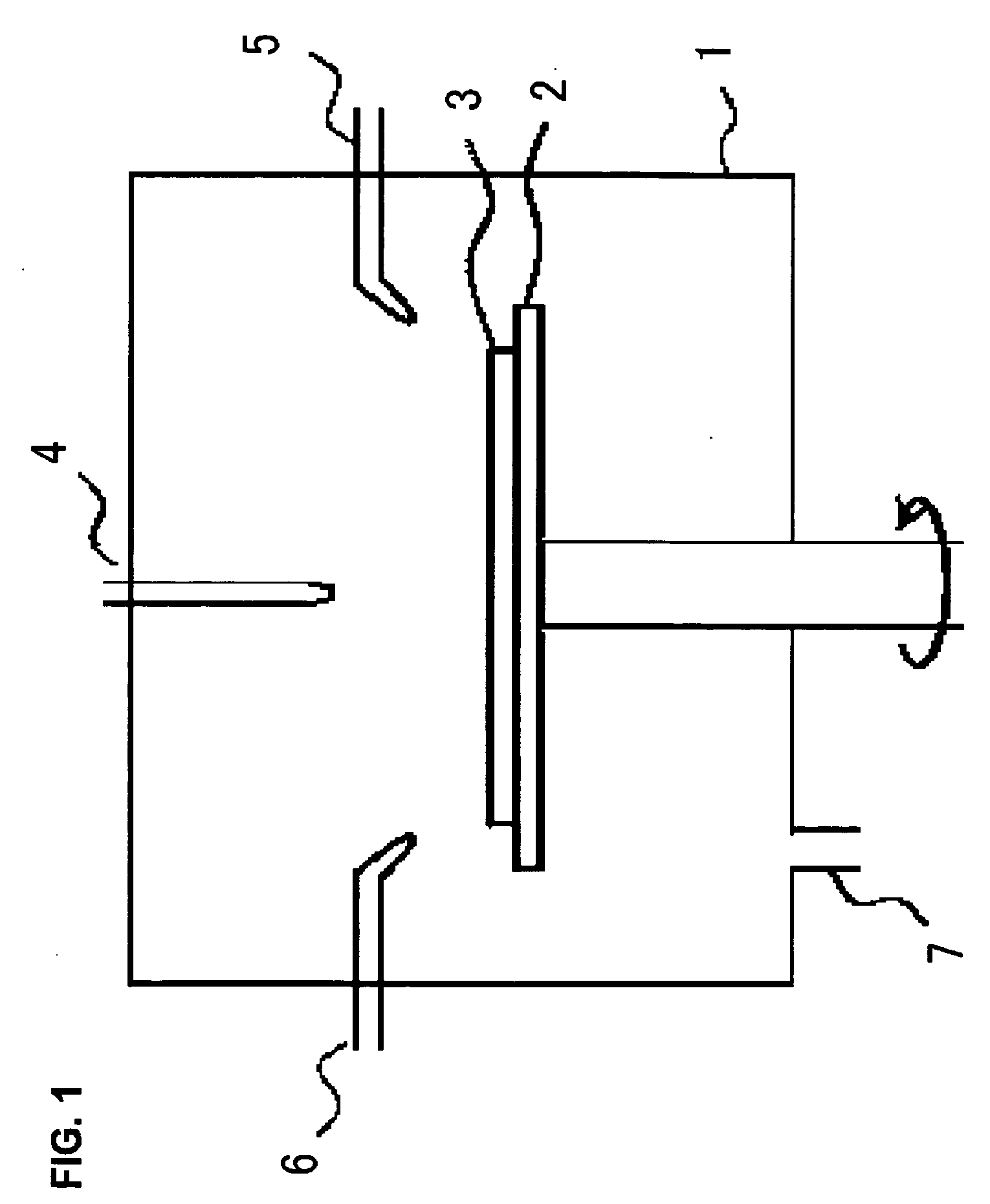
[0099]FIG. 11 is a view showing outline constitution of a substrate treatment device 100 according to the present embodiment. This substrate treatment device 100 is provided with a treatment chamber 102 including a substrate mounting table 104, a first container 126 accommodating a first liquid supplied to the surface of the semiconductor substrate 106, a second container 130 accommodating a second liquid supplied to the semiconductor substrate 106, a mixing part 114, which is communicated with the first container 126 and the second container 130, producing mixture while mixing the first and the second liquids supplied from these containers, a nozzle 112, which communicates with a mixing part 114, supplying the mixture to surface of the semiconductor substrate 106, and a piping 115, which connect the mixing part 114 with the nozzle 112, introducing the mixture from the mixing part 114 to the nozzle 112. In periphery of the piping 115, piping heater 160 heating the piping 115 is disp...

second embodiment

[0135] The present embodiment shows an example providing two nozzles spraying mixture to the semiconductor substrate 106. FIG. 14 is a view showing one example of the substrate treatment device 100 according to the present embodiment, and FIGS. 15A, 15B are views showing position relationship between nozzles 112a, 112b shown in FIG. 14 and the semiconductor substrate 106. Device structure of the present embodiment is the same as the device structure indicated in the first embodiment other than the nozzle structure. The point arranging the heater around the piping 115 and the nozzles 112 is the same as that indicated in the first embodiment.

[0136] As shown in FIGS. 15A, 15B the nozzle 112a sprays the mixture to the end part of the semiconductor substrate 106, and the nozzle 112b sprays the mixture to the center part of the semiconductor substrate 106. The nozzles are prepared at the angle “a” to the substrate surface and at the angle “b” to the direction of the substrate tangent.

[0...

third embodiment

[0139] In the present embodiment, indicated is an example in which the mixture is made to spray to the semiconductor substrate 106. FIG. 16 is a view showing one example of the substrate treatment device 100 according to the present embodiment. Device structure of the present embodiment is the same as the device structure indicated in the first embodiment other than the nozzle structure. The point arranging the heater around the piping 115 and the nozzles 112 shown in FIG. 17 is the same as that indicated in the first embodiment. As shown in the drawing, in this device, the nozzle 112 becomes movable because of control of a moving part 140. The nozzle 112 is constituted so as to spray the mixture while moving a sprayed portion from substrate center to periphery part. In such a constitution as above, within treatment surface of the semiconductor substrate 106, temperature becomes even, as a result, resist stripping efficiency becomes even. Although the present embodiment is one in wh...


PUM

PropertyMeasurementUnit
widthaaaaaaaaaa
heightaaaaaaaaaa
thicknessaaaaaaaaaa

Abstract

A method for manufacturing a semiconductor device and a cleaning device for stripping resist provide semiconductor device with superior element characteristic in a sufficient yield, in such away that, after dry etching of the lithography process, wet cleaning removes resists, and particles or metal impurities are made to sufficiently remove without damaging fine pattern. The method for manufacturing the semiconductor device comprises: forming a resist pattern on a film provided for the semiconductor substrate, forming a fine pattern of conductive film while performing dry etching using the resist pattern as a mask, stripping the resist pattern by single-wafer system treatment upon supplying resist stripping liquid to fine pattern forming surface of the semiconductor substrate, and carrying out rinse treatment of the semiconductor substrate.

Description

[0001] This application is based on Japanese patent applications NO.2003-394249 and NO.2004-324601, the contents of which are incorporated herein by reference. BACKGROUND OF THE INVENTION [0002] 1. Field of the Invention [0003] The present invention relates to a method for manufacturing a semiconductor device and a cleaning device stripping resist using the same method. [0004] 2. Related Art [0005] Conventionally, in the manufacturing of the semiconductor device, a fine pattern formation of a gate electrode or the like is carried out in such a way that a resist film is formed on a conductive film provided on a semiconductor substrate, followed by carrying out dry etching with a resist pattern of the resist film obtained by patterning it as a mask, and the conductive film is subjected to patterning into predetermined size and shape. And, as one technique of resist stripping after the patterning, carried out is a so-called SPM cleaning using mixed solution of sulfuric acid and hydroge...

Claims


Application Information

Patent Timeline
Patent Type & Authority Applications(United States)
IPC IPC(8): G03F7/00G03F7/16H01L29/423G03F7/42H01L21/00H01L21/027H01L21/304H01L21/311H01L29/49
CPCG03F7/162H01L21/31133G03F7/423G03F7/422
Inventor SHIMIZU, YUJISUZUKI, TATSUYAKOHNO, MICHIHISA
Owner NEC ELECTRONICS CORP
Why Eureka
Try Eureka