Process and system for laser annealing and laser-annealed semiconductor film

a laser annealing and semiconductor film technology, applied in the direction of laser beam welding apparatus, solid-state devices, manufacturing tools, etc., can solve the problems of deterioration of tft element characteristics, difficult to transform amorphous semiconductor film into monocrystals, increase in crystallinity, etc., to increase the crystallinity of the predetermined area, increase the effect of crystallinity

Inactive Publication Date: 2007-10-25
FUJIFILM CORP
View PDF4 Cites 1 Cited by
  • Summary
  • Abstract
  • Description
  • Claims
  • Application Information

AI Technical Summary

Benefits of technology

[0034] Therefore, according to the present invention, even in the case where a plurality of bands of crystal grains are grown in directions perpendicular to the scanning direction during the scanning with the laser light, the growing crystals are weeded out and generation of crystal nuclei is suppressed before the scanning reaches the predetermined area the crystallinity of which is to be increased. Therefore, it is possible to grow a large crystal grain from the suppressed number of crystal nuclei in the predetermi

Problems solved by technology

However, according to the conventional laser annealing techniques in which the entire surface of an amorphous semiconductor film is uniformly annealed, the increase in the crystallinity is limited, and it is difficult to transform the amorphous semiconductor film into a monocrystal.
However, when a grain boundary exists in an area in which a TFT element is formed, the characteristics of the TFT element deteriorate.
However, the technique disclosed in Japan

Method used


Image

  • Process and system for laser annealing and laser-annealed semiconductor film
  • Process and system for laser annealing and laser-annealed semiconductor film
  • Process and system for laser annealing and laser-annealed semiconductor film

Examples


Embodiment Construction

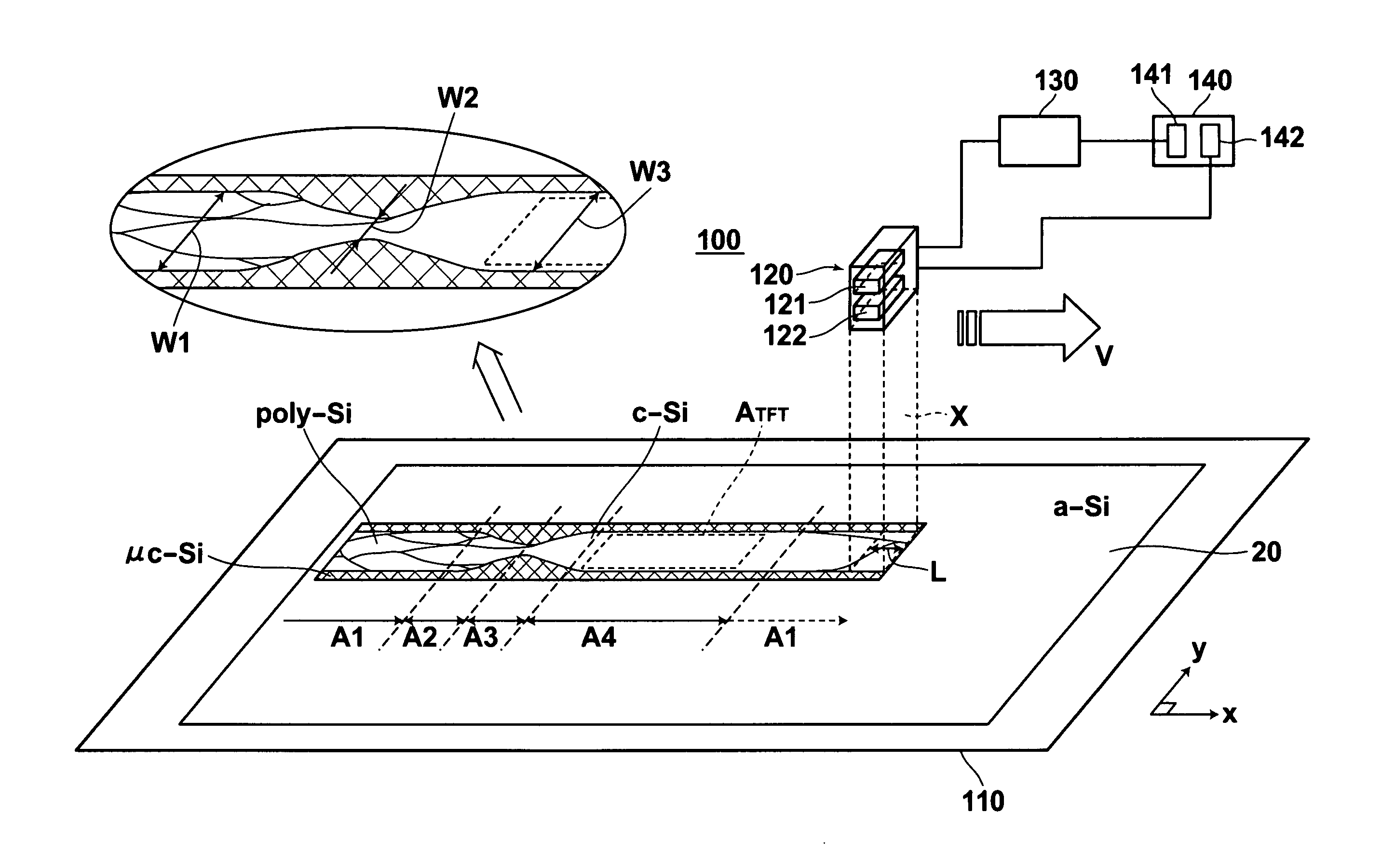
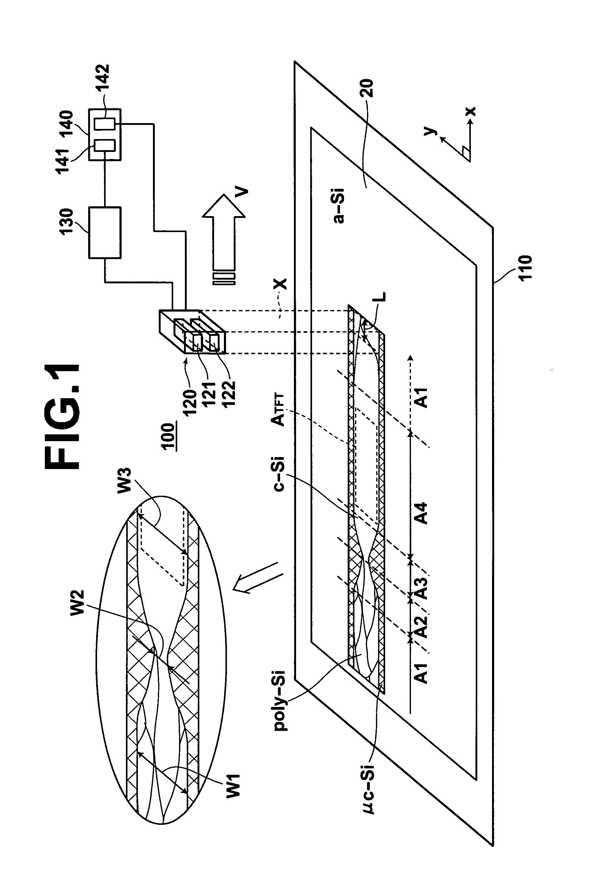
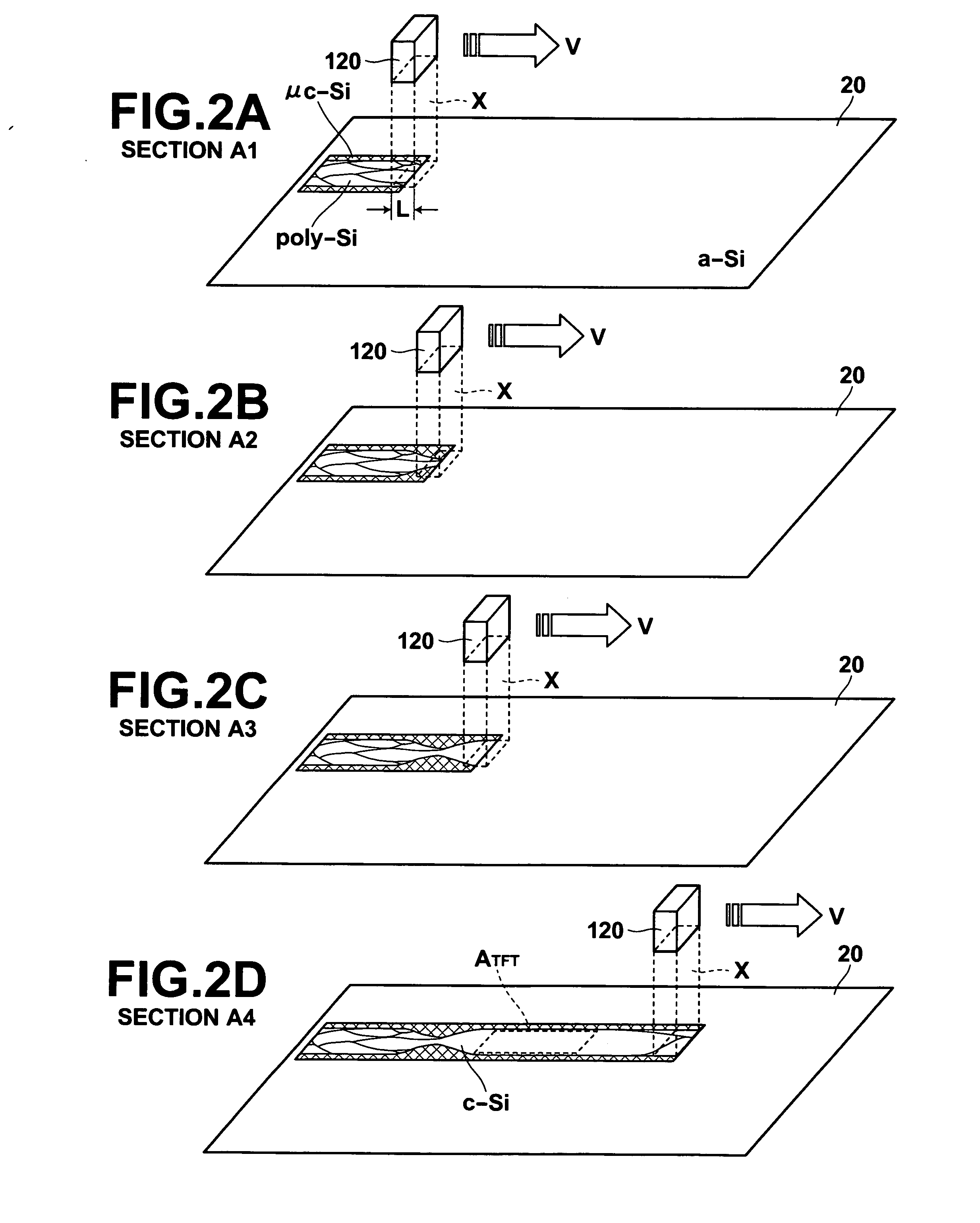
[0047] Preferred embodiments of the present invention are explained in detail below with reference to drawings. In the case which is taken as an example in the following explanations, an active-matrix substrate for use in an active-matrix type electro-optic device such as an electroluminescence (EL) device or a liquid crystal device is produced. In the active-matrix substrate, for example, a great number of thin-film transistors (TFTs) are arranged in a predetermined pattern in correspondence with a great number of pixel electrodes arrayed in a matrix. One or more TFTs are arranged for each pixel. In the case where circuit areas in which driver circuits and the like are formed are arranged around the pixel area in which the pixel electrodes are formed for image display or the like, TFTs may also be formed in the circuit areas.

[0048] Laser Annealing System

[0049] First, the laser annealing system according to an embodiment of the present invention is explained below.

[0050] The lase...


PUM

PropertyMeasurementUnit
Poweraaaaaaaaaa
Widthaaaaaaaaaa
Areaaaaaaaaaaa

Abstract

In a laser annealing process: the first to fourth sections of a bandlike area of a nonmonocrystalline semiconductor film are consecutively scanned and irradiated with laser light so as to produce a fused region in the bandlike area, where the fourth section contains a portion required to have higher crystallinity than other portions of the bandlike area. In the first section, the width of the fused region is substantially uniform. In the second section, the width of the fused region is stepwise or continuously decreased from the width of the fused region in the first section. In the third section, the width of the fused region is stepwise or continuously increased from the width of the fused region at the boundary between the second and third sections. In the fourth section, the width of the fused region at the boundary between the third and fourth sections is substantially uniformly maintained.

Description

BACKGROUND OF THE INVENTION [0001] 1. Field of the Invention [0002] The present invention relates to a laser annealing process and a laser annealing system which irradiate a nonmonocrystalline semiconductor film with laser light so as to increase crystallinity of the nonmonocrystalline semiconductor film. In addition, the present invention also relates to a semiconductor film produced by use of the above laser annealing process or laser annealing system. Further, the present invention relates to a semiconductor device and an electro-optic device using the above semiconductor film. [0003] 2. Description of the Related Art [0004] Currently, the active-matrix type driving systems are widely used in the electro-optic devices such as the electroluminescence (EL) devices and the liquid crystal (display) devices in which an image is displayed by dot-by-dot driving. In the active-matrix type driving systems, a great number of pixel electrodes arrayed in a matrix are driven through switching...

Claims


Application Information

Patent Timeline
IPC IPC(8): H01L21/20
CPCB23K26/0732H01L21/2026H01L27/1296H01L27/1285H01L27/1214H01L21/02683H01L21/02686H01L21/02422H01L21/02488H01L21/02532H01L21/02691H01L21/324H01L21/477
Inventor TANAKA, ATSUSHI
Owner FUJIFILM CORP
Why Eureka
Try Eureka