Liquid crystal display unit

Inactive Publication Date: 2005-07-28
VISTA PEAK VENTURES LLC
View PDF8 Cites 11 Cited by
  • Summary
  • Abstract
  • Description
  • Claims
  • Application Information

AI Technical Summary

Benefits of technology

[0012] The present invention has been devised in view of such circumstances, and a primary object of the present invention is to provide an active matrix liquid crystal display unit in which a break of wiring at the intersection of lower wiring (gate wiring) and upper wiring (drain wiring) is prevented with reliability.
[0017] In this way, in the liquid crystal display unit according to the present invention, the recesses formed in the first wiring (gate wiring) on the TFT substrate adequately elongate the etchant penetration path, and thus, even if the width of the drain wiring is small, a break of the drain wiring can be prevented with reliability. In addition, since the gate wiring is composed of two layers of Mo and Al, and the side faces of the gate wiring are tapered, the step on the drain wiring can be made less steep, and deterioration in quality and reduction in thickness of the drain wiring at the step can be suppressed. As a result, the etchant penetration is hard to occur, and thus, a break of the drain wiring can be prevented with higher reliability.

Problems solved by technology

Furthermore, sputtering cannot provide adequate step coverage, and thus, the resulting metal film, which is to constitute the drain wiring 6, is thinner on the side faces of the step on the gate insulating film 3 formed due to the gate wiring 2.
As a result, a problem occurs that the drain wiring 6 is broken.
As the drain wiring becomes thinner, the penetration path for the etchant becomes shorter, and the wire becomes more likely to be broken.
The protrusions formed on the gate wiring 2 described in the Japanese Patent Laid-Open No. 8-330592 cannot provide sufficient extension of the penetration path for the etchant.
At the side faces of the step, the metal film is covered inadequately, so that the metal film is thinner than in the remaining areas, and thus, the metal film is susceptible to penetration of the etchant.
Thus, even if the protrusions are formed on the gate wiring 2 to elongate the penetration path for the etchant, it is difficult to prevent the drain wiring 6 from being broken with reliability.

Method used


Image

  • Liquid crystal display unit
  • Liquid crystal display unit
  • Liquid crystal display unit

Examples


first embodiment

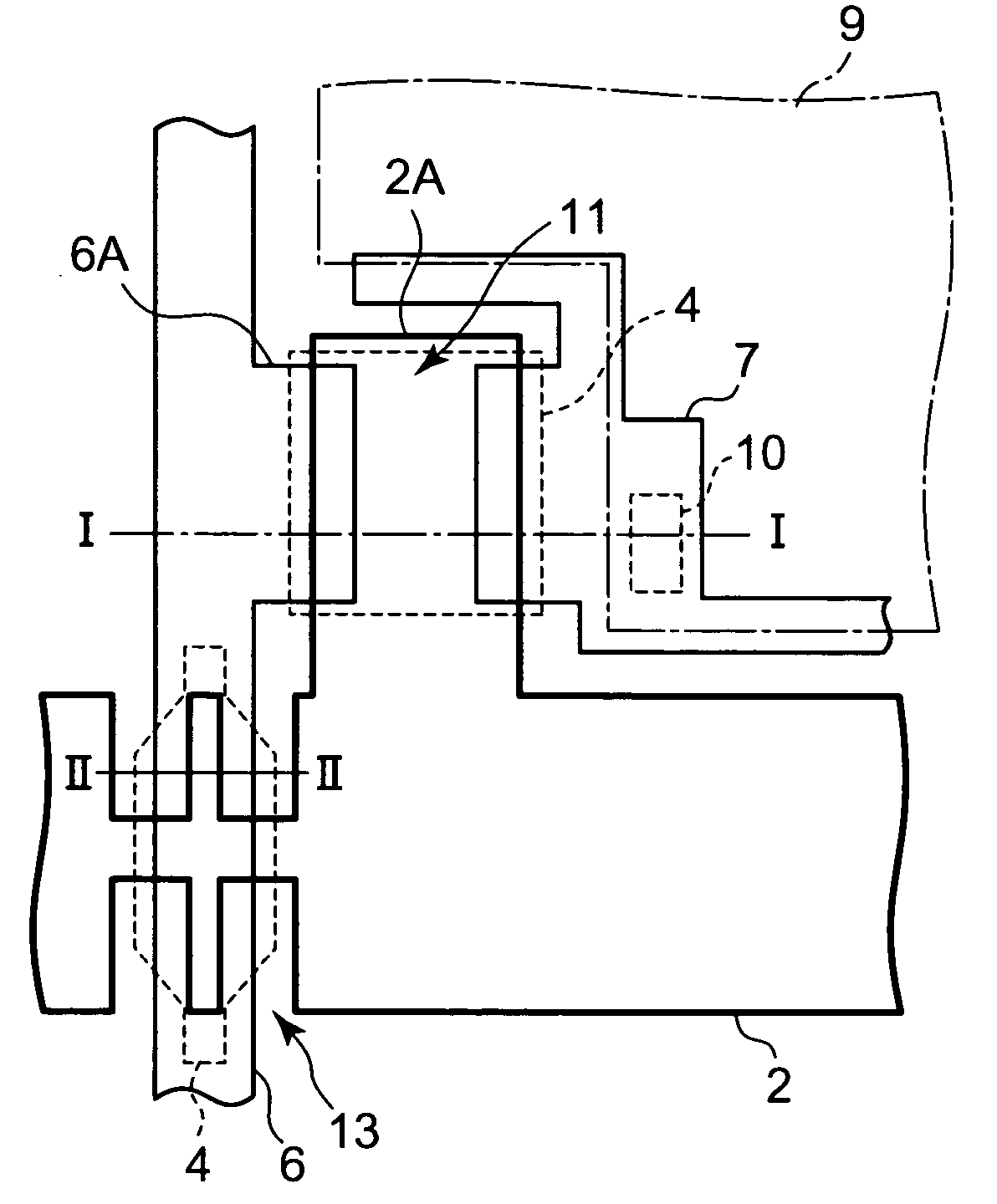
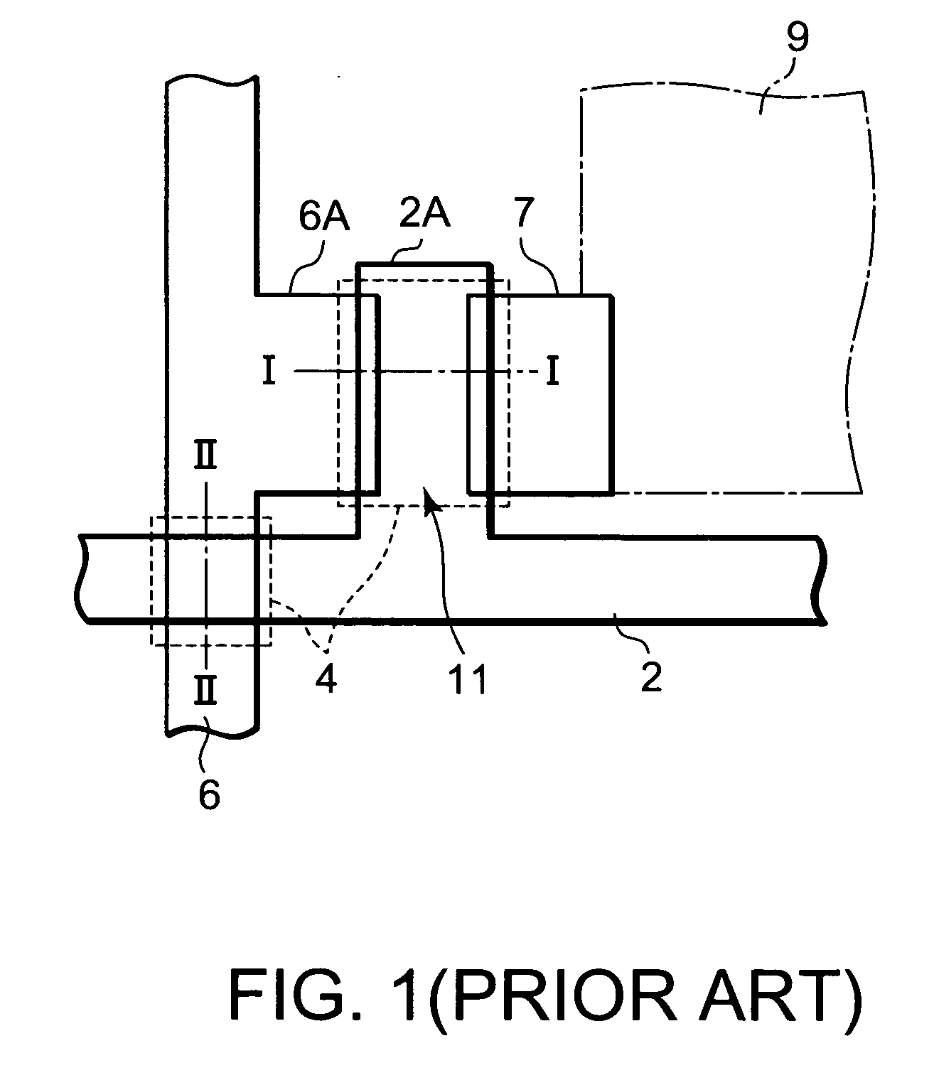
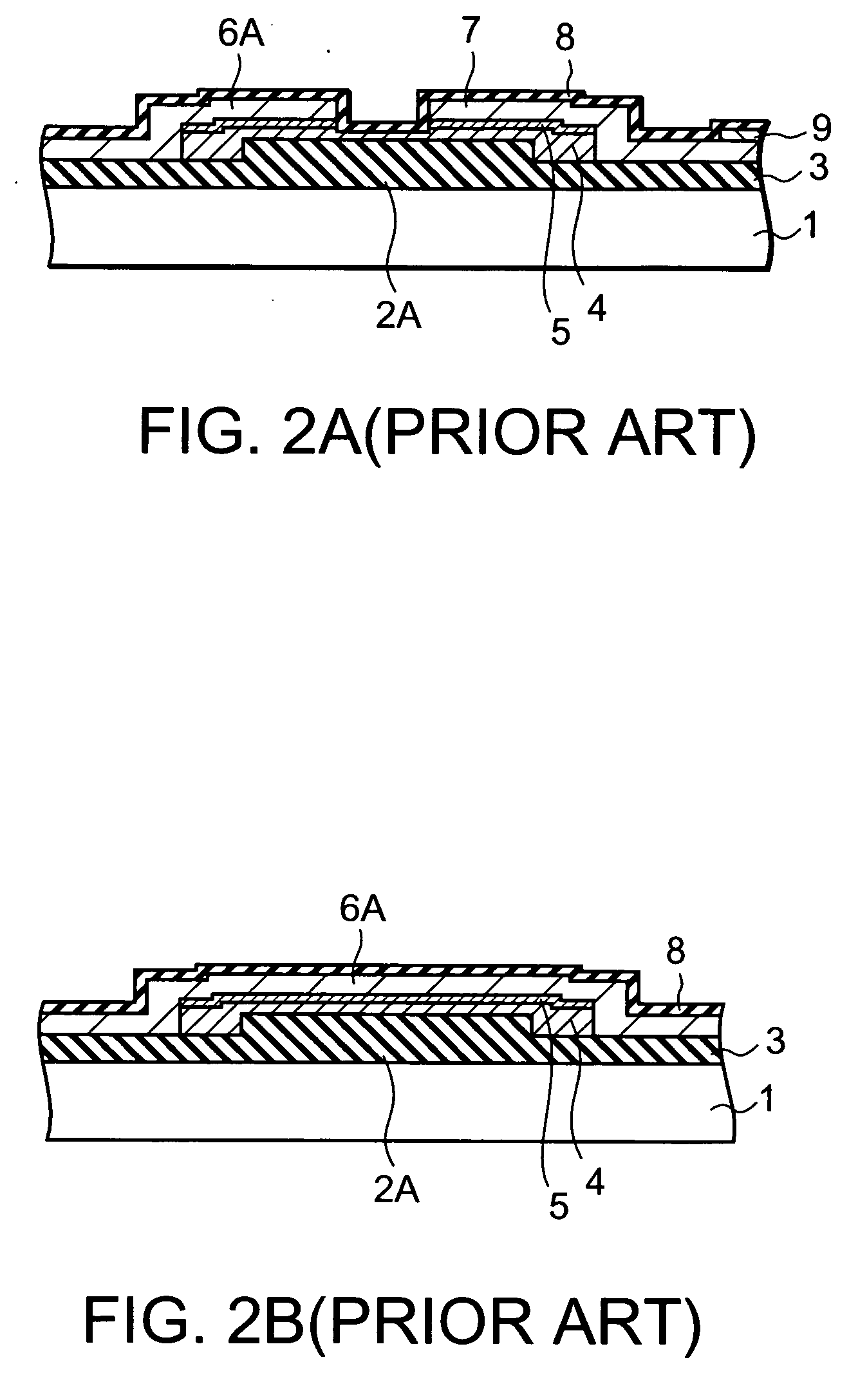
[0047] An active matrix liquid crystal display unit according to a first embodiment will be described with reference to the drawings.

[0048]FIG. 4 is across sectional view of the liquid crystal display unit according to the first embodiment of the present invention.

[0049] Referring to FIG. 4, the liquid crystal display unit according to the first embodiment has a transparent insulating substrate 1, a gate electrode 2A and gate wiring (not shown) formed on the transparent insulating substrate, and a gate insulating film 3 made of silicon nitride formed on the transparent insulating substrate 1 and the gate electrode 2A. The gate electrode 2A and the gate wiring are composed of two layers, one of which is made of Al or an Al alloy, and the other of which is made of Mo or a Mo alloy. On the gate insulating film 3, an island-like semiconductor layer comprising an a-Si sublayer 4 and an n+a-Si sublayer 5. Parts of the n+a-Si sublayer 5 and the a-Si sublayer 4 of the semiconductor layer ...

second embodiment

[0071] In the following, an active matrix liquid crystal display unit according to a second embodiment of the present invention will be described with reference to FIGS. 13 to 16. FIG. 13 is a plan view of a TFT substrate of the liquid crystal display unit according to the second embodiment of the present invention showing a configuration thereof near an intersection of gate wiring and drain wiring. FIG. 14A is a cross-sectional view taken along the line III-III in FIG. 13, and FIG. 14B is a cross-sectional view taken along the line IV-IV in FIG. 13. FIGS. 15A to 15E are cross-sectional views for schematically illustrating steps of a method of fabricating the TFT substrate of the liquid crystal display unit according to the second embodiment of the present invention. FIG. 16 is a graph for illustrating an advantage of the second embodiment.

[0072] In the case of the liquid crystal display unit according to the first embodiment of the present invention described above, the TFT substr...


PUM


Abstract

To provide an active matrix liquid crystal display unit in which a wiring break at the intersection of drain wiring and gate wiring is prevented with reliability. One or more recesses extending along drain wiring and having a depth equal to or greater than the width of the drain wiring are formed in at least one side of gate wiring at an area near an intersection of the gate wiring and the drain wiring. Furthermore, the gate wiring is composed of two layers of Mo and Al, for example, and the side faces of the gate wiring are tapered. The recesses having a sufficient depth formed in the gate wiring at the area near the intersection with the drain wiring adequately elongate the etchant penetration path.

Description

BACKGROUND OF THE INVENTION [0001] 1. Field of the Invention [0002] The present invention relates to a liquid crystal display unit. In particular, it relates to an active matrix liquid crystal display unit. [0003] 2. Description of the Related Art [0004] An active matrix liquid crystal display unit using a thin film transistor (abbreviated as TFT, hereinafter) as a switching element is widely used. Such an active matrix liquid crystal display unit comprises: a substrate on which gate wiring, drain wiring, TFTs, pixel electrodes and the like are disposed (referred to as a TFT substrate, hereinafter); an opposite substrate on which a color filter, a black matrix and the like are disposed; and a liquid crystal interposed between the substrates. Applying a voltage between the electrodes on the TFT substrate and the electrodes on the opposite substrate or between plural electrodes on the TFT substrate causes the orientations of the liquid crystal molecules, thereby controlling the light ...

Claims


Application Information

Patent Timeline
IPC IPC(8): G02F1/1368G02F1/133G02F1/136G02F1/1362H01L21/28H01L21/3213H01L21/336H01L21/77H01L27/12H01L29/786H01L31/036
CPCG02F1/136286H01L27/124H01L27/12G02F1/136
Inventor KIMURA, SHIGERU
Owner VISTA PEAK VENTURES LLC
Why Eureka
Try Eureka