Correlated double sampling circuit, signal processing circuit, and solid-state imaging apparatus

a signal processing circuit and sampling circuit technology, applied in the field of correlation double sampling circuits, signal processing circuits, solid-state imaging apparatuses, can solve the problems of increasing power consumption, affecting the operation of reset noise, and increasing the load of buffer amplifiers, so as to reduce the difference in voltage, reduce power consumption, and reduce the voltage

Inactive Publication Date: 2005-07-28
NEC ELECTRONICS CORP
View PDF3 Cites 7 Cited by
  • Summary
  • Abstract
  • Description
  • Claims
  • Application Information

AI Technical Summary

Benefits of technology

[0028] According to one aspect of the invention, there is provided a correlated double sampling circuit, including a plurality of sampling circuits, each of which samples each of a plurality of color signals sequentially output from a solid-state imaging device. This allows reduction of a difference in the voltage of the color signal sampled by each sampling circuit. A load to an amplifier and so on which supplies a voltage to each sampling circuit thereby decreases, thus achieving lower power consumption.
[0029] According to another aspect of the invention, there is provided a signal processing circuit including an amplifier which amplifies a first color signal and a second color signal sequentially output from a solid-state imaging device, a first sampling circuit which samples the amplified first color signal, a second sampling circuit which samples the amplified second color signal, a first timing regulator which adjusts an output timing of the signal sampled by the first sampling circuit, and a second timing regulator which adjusts an output timing of the signal sampled by the second sampling circuit. This allows reduction of a difference in the voltage of the color signal sampled by each sampling circuit. A load to an amplifier and so on which supplies a voltage to each sampling circuit thereby decreases, thus achieving lower power consumption.
[0030] According to still another aspect of the invention, there is provided a solid-state imaging apparatus including a solid-state imaging device which sequentially outputs a plurality of color signals, a first sampling circuit which samples a first color signal selected from the plurality of color signals, a second sampling circuit which samples a second color signal selected from the plurality of color signals, a first switching circuit which outputs the signal sampled by the first sampling circuit, a second switching circuit which outputs the signal sampled by the second sampling circuit, and an amplifier which amplifies the signal output from the first switching circuit or the second switching circuit. This allows reduction of a difference in the voltage of the color signal sampled by each sampling circuit. A load to an amplifier and so on which supplies a voltage to each sampling circuit thereby decreases, thus achieving lower power consumption.
[0031] The present invention allows reduction of power consumption even if a difference in color signals output from an imaging device is large.

Problems solved by technology

The low power consumption and high speed operation are conflicting goals since higher speed generally requires higher power consumption.
In this process, reset noise occurs in the reset operation after converting a signal charge of one pixel into a voltage.
This results in an increase in a load to the buffer amplifier in the previous stage of the sampling circuit, which increases power consumption.
Furthermore, a circuit which samples a high-frequency signal requires high power, which hinders the achievement of low power consumption.

Method used


Image

  • Correlated double sampling circuit, signal processing circuit, and solid-state imaging apparatus
  • Correlated double sampling circuit, signal processing circuit, and solid-state imaging apparatus
  • Correlated double sampling circuit, signal processing circuit, and solid-state imaging apparatus

Examples


first embodiment

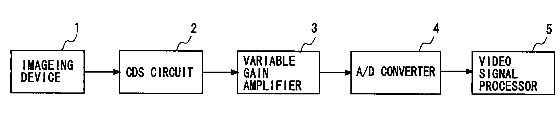
[0046] Referring first to FIG. 1, the structure of a solid-state imaging apparatus according to a first embodiment of the invention is explained. The solid-state imaging apparatus includes an imaging device 1, a CDS circuit 2, a variable gain amplifier 3, an A / D converter 4, and a video signal processor 5. These components may be integrated in one chip or may be formed in a given number of chips. For example, the CDS circuit 2, the variable gain amplifier 3 and the A / D converter 4 may be integrated in one chip. Further, all the components may be included in one solid-state imaging apparatus, or, if the video signal processor 5 is configured by a personal computer (PC), it maybe configured as a separate apparatus from the solid-state imaging apparatus.

[0047] For example, the imaging device 1 photoelectrically converts light into a signal, and outputs the generated signal to the CDS circuit 2. The CDS circuit 2 removes the noise contained in the output signal. Then, the variable gain...

second embodiment

[0085] Referring now to the circuit diagram of FIG. 8, the configuration of a CDS circuit of a second embodiment of the invention is explained. The CDS circuit 2 of this embodiment has an amplifier VA1 (first color correction circuit) between the sampling circuit SH1 and the output switch SW3, and an amplifier VA2 (second color correction circuit) between the sampling circuit SH2 and the output switch SW5, in addition to the elements shown in FIG. 3.

[0086] The amplifiers VA1 and VA2 may be variable gain amplifiers, for example. The gain of the amplifiers may be varied for each color signal to perform color correction such as white balance.

[0087] The variable gain amplifier of FIG. 5 may be used for the amplifiers VA1 and VA2. In this case, since a different amplifiers are used for a different color signal, the frequency of changing the gain for color correction and so on decreases, which reduces switching noise that can occur at the time of switching to change the gain. For exampl...

third embodiment

[0088] Referring then to the circuit diagram of FIG. 9, the configuration of a CDS circuit of a third embodiment of the invention is explained. In FIG. 9, the same reference symbols as in FIG. 3 designate the same elements.

[0089] The CDS circuit 2 of this embodiment includes a capacitor C1, a DC regeneration circuit DC1, a buffer amplifier BA1, sampling circuits SH1 and SH2, a sampling circuit SH3 (third sampling circuit), and a sampling circuit SH4 (third timing regulator or fourth sampling circuit). The capacitor C1 receives the output signal from the imaging device 1. The DC regeneration circuit DC1 regenerates a direct-current component. The buffer amplifier BA1 amplifies the DC-regenerated signal. The sampling circuits SH1 and SH2 sample the signal in the color signal period. The sampling circuit SH3 samples the signal in the reference period. The sampling circuit SH4 matches the phases of the sampling signals in the reference period by regulating signal output timing. The var...


PUM


Abstract

The correlated double sampling circuit includes a plurality of sampling circuits. Each of the sampling circuits samples each of a plurality of color signals which are sequentially output from a solid-state imaging device.

Description

BACKGROUND OF THE INVENTION [0001] 1. Field of the Invention [0002] The present invention relates to correlated double sampling circuits, signal processing circuits, and solid-state imaging apparatus. Particularly, the invention relates to the correlated double sampling circuit, signal processing circuit, and solid-state imaging apparatus which process a signal from a color solid-state imaging device. [0003] 2. Description of Related Art [0004] Recent solid-state imaging apparatus such as a digital camera include a solid-state imaging device with high pixel density. The solid-state imaging device is a charge coupled device (CCD), for example. Further, higher speed devices with lower power consumption are needed. The low power consumption and high speed operation are conflicting goals since higher speed generally requires higher power consumption. [0005] In a solid-state imaging device, a plurality of photo-detectors composed of photodiode and so on photoelectrically convert light in...

Claims


Application Information

Patent Timeline
Patent Type & Authority Applications(United States)
IPC IPC(8): H04N5/335H04N5/357H04N5/363H04N5/378H04N9/07
CPCH04N5/378H04N25/75
Inventor MATSUI, TAKEO
Owner NEC ELECTRONICS CORP
Why Eureka
Try Eureka