

Liquid crystal display element, and liquid crystal display device
a liquid crystal display element and liquid crystal display technology, applied in non-linear optics, instruments, optics, etc., can solve the problems of low contrast, adversely affecting the v-t (drive voltage-transmittance curve), and the reflectance of the reflection pixel electrodes covered with silicon dioxide is not uniform in the whole waveband, so as to prevent color balance and high reflectance
- Summary
- Abstract
- Description
- Claims
- Application Information
AI Technical Summary
Benefits of technology
Problems solved by technology
Method used
Image

Examples
Embodiment Construction
[0059] The present invention will be described in detail below concerning a liquid crystal display element and liquid crystal display device with reference to the accompanying drawings.
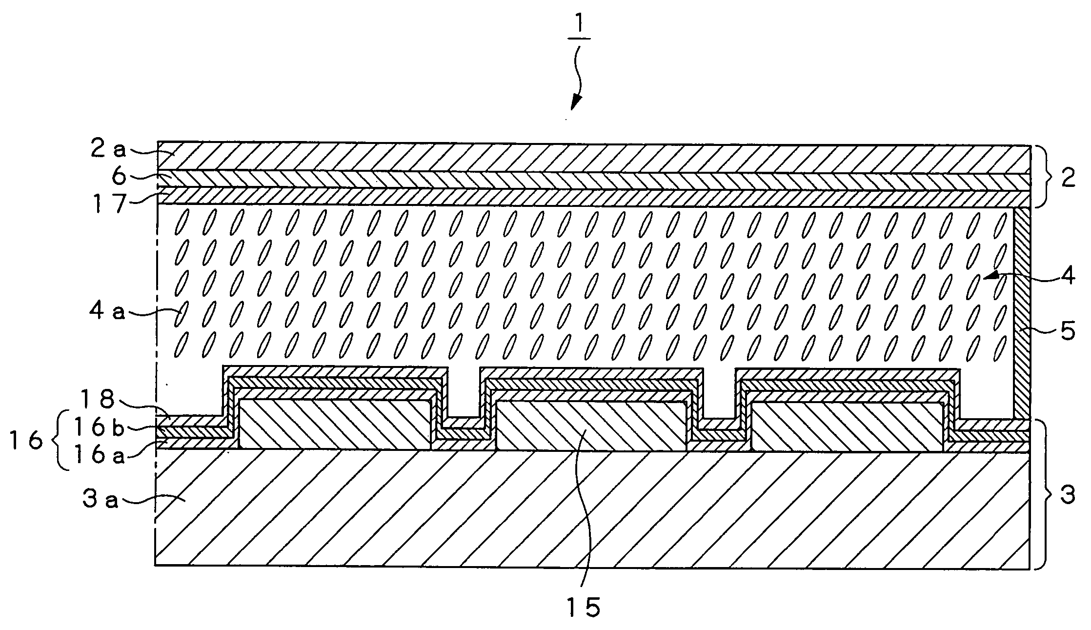
[0060] Referring now to FIG. 7, there is schematically illustrated a reflection type liquid crystal element of an active type according to the present invention in the form of a sectional view. The reflection type liquid crystal display element is generally indicated with a reference numeral 1. It should be noted that for easier understanding of the features of the reflection type liquid crystal display element 1, the characterizing portions are illustrated on an enlarged scale and hence all the portions are not shown at the same scale ratio in FIG. 7 as the one used in the actual element.
[0061] As shown, the reflection type liquid crystal display element 1 includes a transparent substrate 2 and drive circuit board 3, disposed opposite to each other, a liquid crystal layer 4 interposed between the t...
PUM
| Property | Measurement | Unit |
|---|---|---|
| thickness | aaaaa | aaaaa |
| thickness | aaaaa | aaaaa |
| pretilt angle | aaaaa | aaaaa |
Abstract
Description
Claims
Application Information