
Vapor-phase epitaxial apparatus and vapor phase epitaxial method

a growth apparatus and vapor phase technology, applied in the direction of polycrystalline material growth, crystal growth process, chemically reactive gas growth, etc., can solve the problems of difficult conventional vapor phase growth apparatus, and achieve the effect of equilibrating the heat resistance of individual heat transfer routes

Inactive Publication Date: 2005-08-04
JX NIPPON MINING& METALS CORP
View PDF11 Cites 3 Cited by
  • Summary
  • Abstract
  • Description
  • Claims
  • Application Information

AI Technical Summary

Benefits of technology

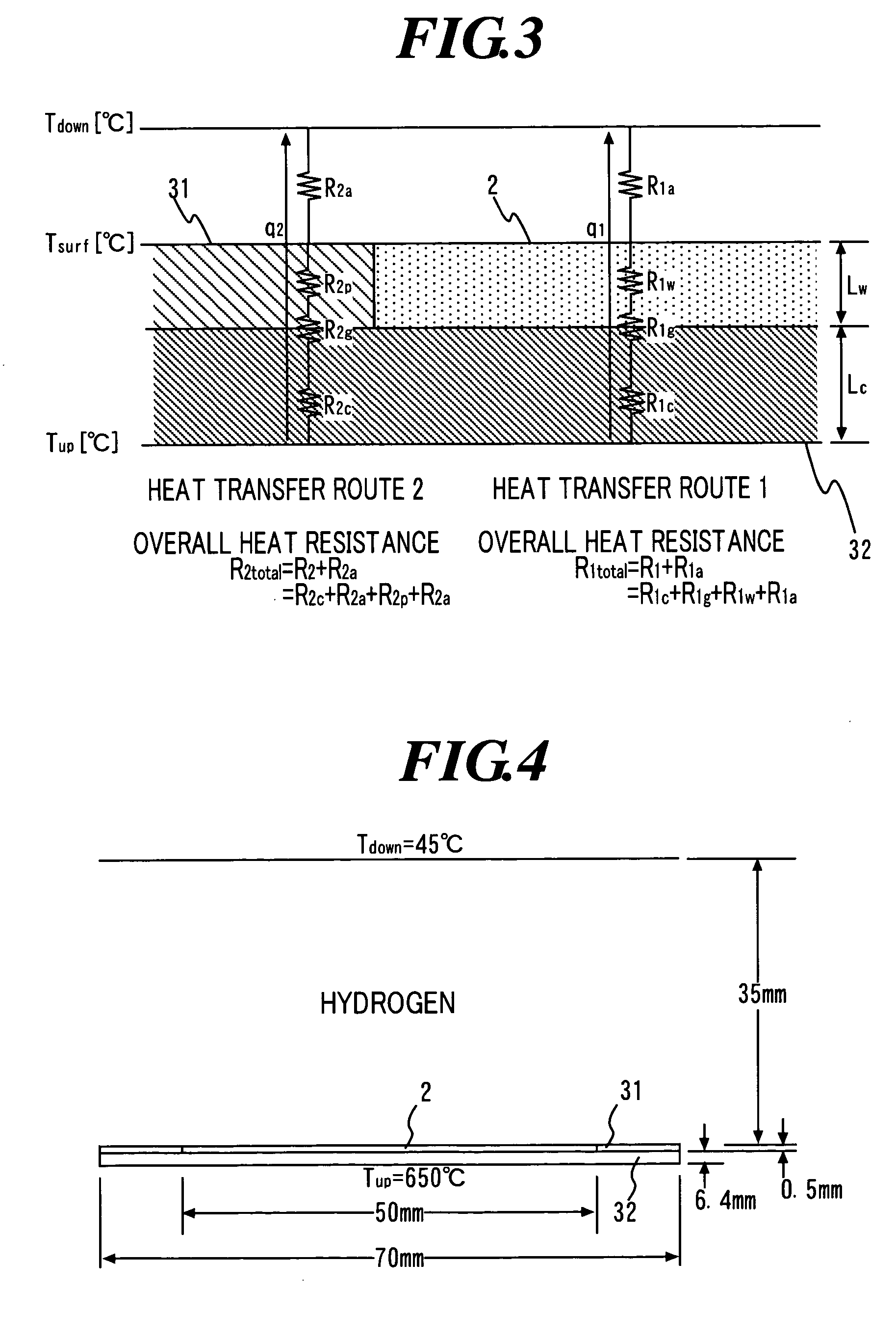
[0010] According to the wafer container having such a structure, it is possible to adjust the ratio R2 / R1 easily, where R1 is a heat resistance in a heat transfer route from a rear surface of the heat flow transmitting section to the front surface of the wafer, and R2 is a heat resistance in a heat transfer route from the rear surface of the heat flow transmitting section to a front surface of the heat flow control section.
[0012] This almost equalizes the heat resistances in the individual heat transfer routes each other and thus ensures similar heat transfer during heat transfer from the rear surface of the wafer container (the rear surface of the heat flow transmitting section) toward the front surfaces of the wafer and of the wafer container (the front surface of the heat flow control section), and this consequently equalizes achievable temperatures of the surfaces of the wafer and the wafer container. This successfully prevents the surface temperature at the circumferential portion of the wafer from rising higher than the surface temperature at the center of the wafer, which is caused by temperature difference between the surfaces of the wafer and the wafer container. Thus, it becomes possible to keep a uniform in-plane temperature distribution of the wafer. As a consequence, a thin film having a desirable uniformity can grow in the vapor phase over the entire surface of the wafer.
[0013] The heat resistance Rg is not less than 1.0×10⁻⁶ m2K / W and not more than 5.0×10⁻³ m2K / W; otherwise a clearance distance between the heat flow control section and the heat flow transmitting section may be approximately uniform and in a range of 0.001 mm to 1 mm. Accordingly, because the heat resistance Rg comes to be approximately equal to the contact heat resistance between the heat flow transmitting section and the wafer, it is possible to adjust the ratio R2 / R1 easily.
[0041] That is, it is possible to bring near the heat resistance values R1 and R2 to each other, by bringing the value of contact heat resistance Rig between the wafer 2 and the heat flow transmitting section 32 near the value of contact heat resistance R2g between the heat flow control section 31 and the heat flow transmitting section 32 and also by bringing the value of coefficient of thermal conductivity k1w of the wafer 2 near the value of coefficient of thermal conductivity k2p of the heat flow control section 31.

Problems solved by technology

In other words, it was found to be difficult for the conventional vapor-phase growth apparatus 100 to form a thin film with a high uniformity over the entire surface of the wafer 2 by vapor-phase growth since in-plane temperature distribution of the wafer 2 could not be uniform.

Method used


Image

  • Vapor-phase epitaxial apparatus and vapor phase epitaxial method
  • Vapor-phase epitaxial apparatus and vapor phase epitaxial method
  • Vapor-phase epitaxial apparatus and vapor phase epitaxial method

Examples


Embodiment Construction

[0055] An embodiment of the vapor-phase growth apparatus (MOCVD apparatus) of the present invention will be described below referring to the attached drawings.

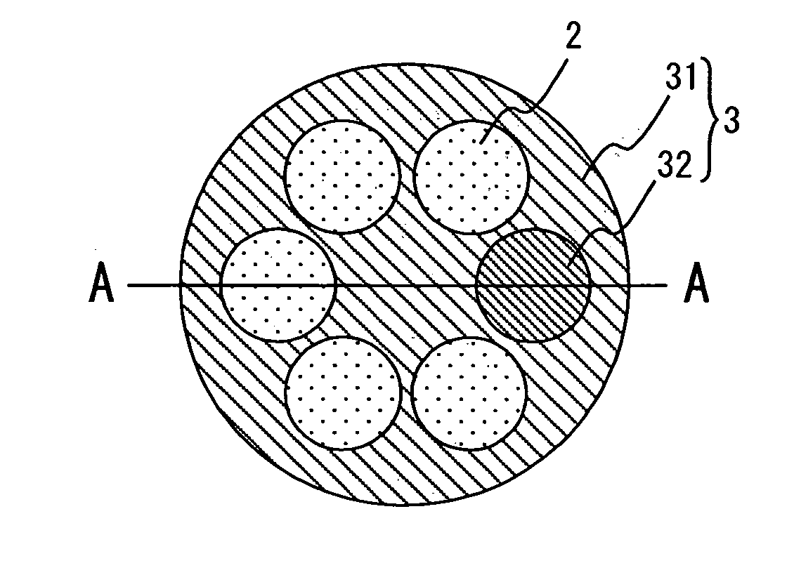
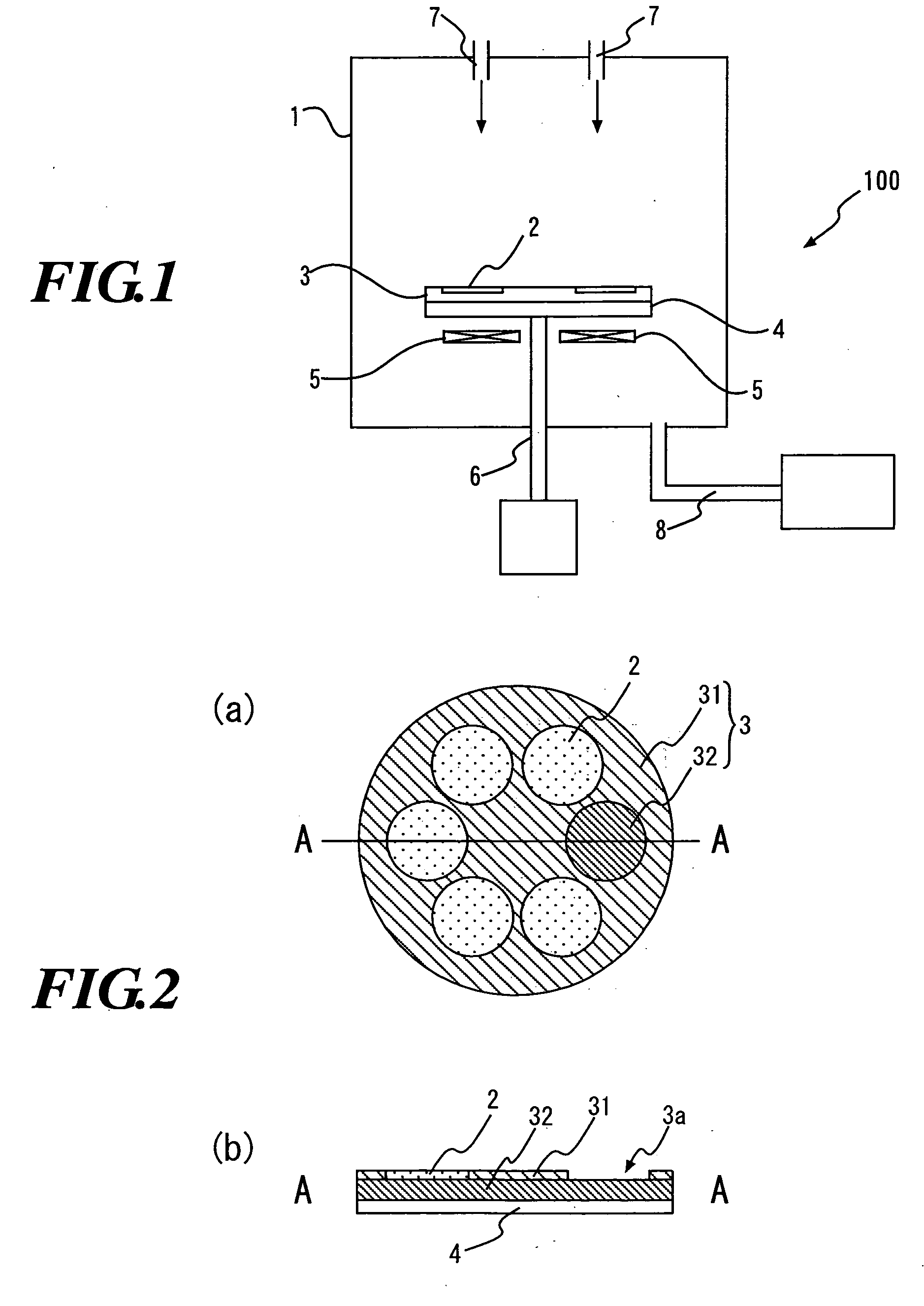
[0056]FIG. 1 is a sectional view showing a schematic construction of the vapor-phase growth apparatus according to the present embodiment. FIG. 2 is an enlarged view showing a detailed construction of the wafer holder 3 in the present invention, where (a) is a plan view, and (b) is a sectional view taken along the line A-A.

[0057] In the earlier development, the wafer holder 3 which is a wafer container was made of a material having a large coefficient of thermal conductivity, such as graphite. The vapor-phase growth apparatus of the embodiment is different from the earlier development in that the wafer container comprises: a heat flow transmitting section 32 made of a material having a large coefficient of thermal conductivity, such as graphite; and a heat flow control section 31 made of amorphous carbon (abbreviated as a-ca...


PUM

PropertyMeasurementUnit
Temperatureaaaaaaaaaa
Lengthaaaaaaaaaa
Lengthaaaaaaaaaa

Abstract

A vapor-phase growth apparatus includes: a reaction furnace which is hermetically closable, a wafer container which is disposed in the reaction furnace, for disposing a wafer at a predetermined position, a gas supply member for supplying a source gas toward the wafer, and a heating member for heating the wafer, wherein the apparatus is designed to form a grown film on a front surface of the wafer by supplying the source gas in a high temperature state while the heating member heats the wafer in the reaction furnace through the wafer container. The wafer container includes: a heat flow control section having a space for disposing a wafer; and a heat flow transmitting section joined to the heat flow control section, for transmitting heat to the wafer disposed in the space; and contact heat resistance Rg between the heat flow control section and the heat flow transmitting section is not less than 1.0×10⁻⁶ m2K / W to not more than 5.0×10⁻³ m2K / W, and the heat flow control section is made of a material having a coefficient of thermal conductivity which is not less than 5 times to not more than 20 times that of the wafer disposed on the heat flow transmitting section.

Description

TECHNICAL FIELD [0001] The present invention relates to a vapor-phase growth apparatus and a vapor-phase growth method, for growing a thin film of compound semiconductor or the like on a surface of a wafer in a vapor phase, while heating the wafer under a supply of a source gas in a high temperature state, and in particular to material characteristics of a wafer container for disposing wafers thereon. BACKGROUND ART [0002] Vapor-phase growth process is currently utilized in various industrial fields. Needless to say, in the vapor-phase growth, advanced uniformities in thickness, composition and doping concentration of a film grown on the wafer over the entire surface thereof are essential matters. Achievement of thermal uniformity in wafer heating is therefore recognized as the most important elementary technology as one means for realizing the aforementioned uniformities over the entire surface. [0003]FIG. 1 is a sectional view showing an exemplary constitution of a general vapor-p...

Claims


Application Information

Patent Timeline
IPC IPC(8): C23C16/46C30B25/10C30B25/12H01L21/205
CPCC23C16/46C30B25/10C30B25/12Y10T117/1008Y10T117/1012Y10T117/1004Y10T117/1016
Inventor SHIMIZU, EIICHIMAKINO, NOBUHITO
Owner JX NIPPON MINING& METALS CORP
Learn More