Stereoscopic electronic circuit device, and relay board and relay frame used therein

a technology of electronic circuit device and relay frame, which is applied in the direction of printed circuit non-printed electric components association, sustainable manufacturing/processing, and final product manufacturing, etc., can solve the problems of preventing an improvement in mounting density, limiting the improvement of mounting density in two-dimensional electronic circuit device, and the inability to completely shield the radiation of unnecessary electromagnetic waves or the intrusion of external noise through the gaps of corner posts

Inactive Publication Date: 2005-08-04
PANASONIC CORP
View PDF5 Cites 105 Cited by
  • Summary
  • Abstract
  • Description
  • Claims
  • Application Information

AI Technical Summary

Problems solved by technology

However, while electronic devices are becoming higher performing and miniaturized, there is a limit to improving mounting density in two-dimensional electronic circuit devices only by reducing the interconnection pitch to a micro level or decreasing the spacing between adjacent components.
Thus the increase in the area for the connection between the module circuit boards prevents an improvement in mounting density.
However, such shielding with a metal case or an insulating metal board for EMC measurements in line with high-speed and high-frequency electronic devices has the following problems.
In addition, it is impossible to completely shield the radiation of unnecessary electromagnetic waves or the intrusion of external noise through the gaps of the corner posts because these are where the top and bottom insulating metal boards are connected with each other.

Method used


Image

  • Stereoscopic electronic circuit device, and relay board and relay frame used therein
  • Stereoscopic electronic circuit device, and relay board and relay frame used therein
  • Stereoscopic electronic circuit device, and relay board and relay frame used therein

Examples


first embodiment

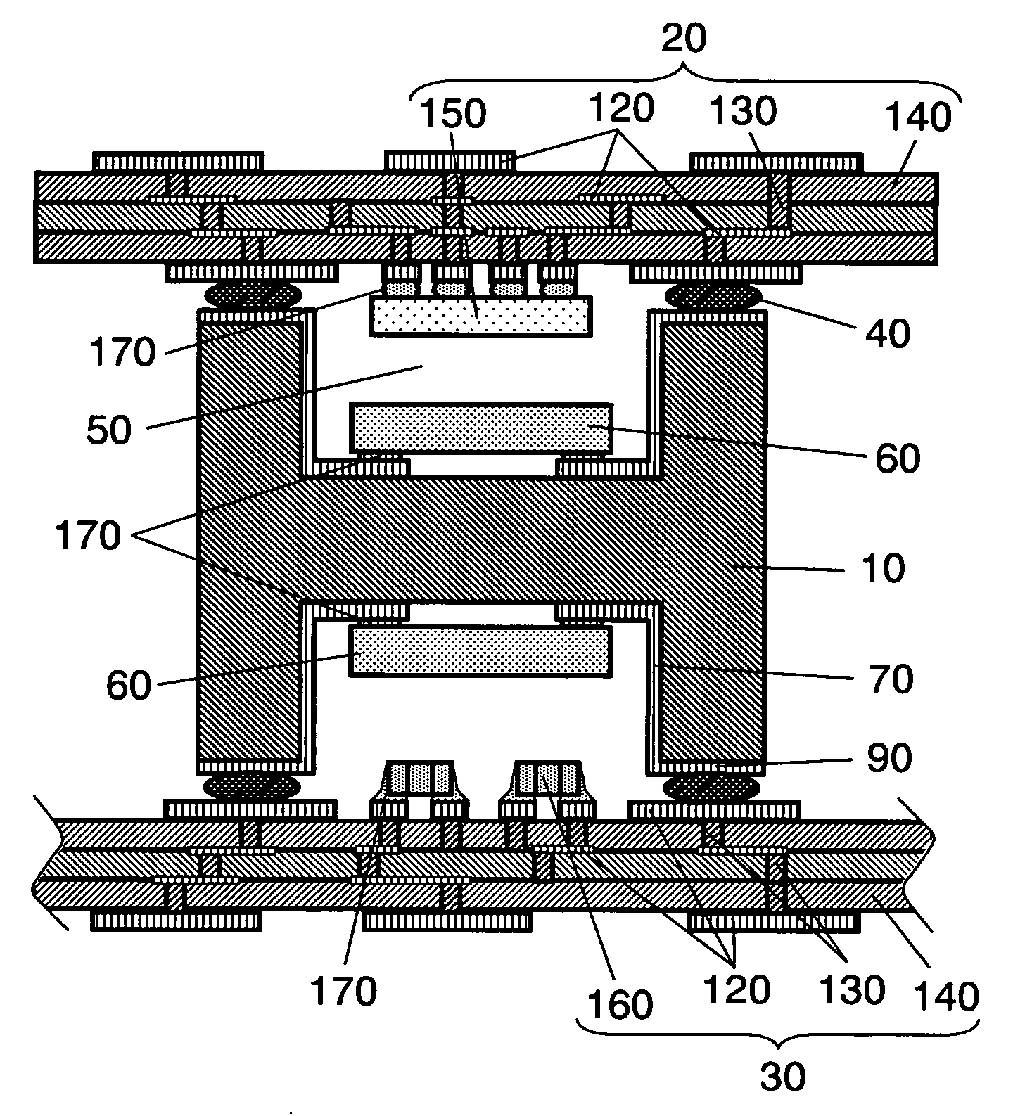
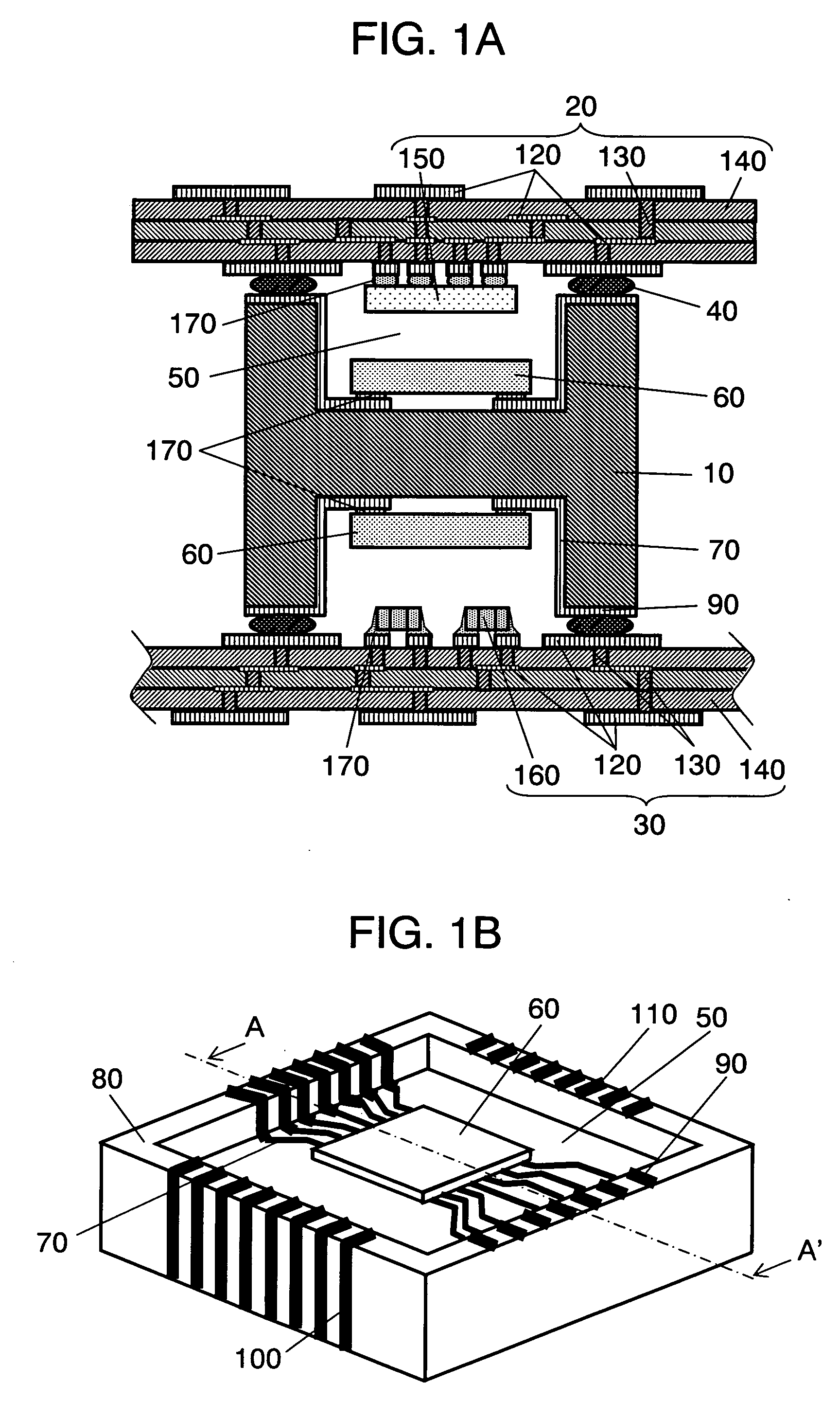
[0081]FIGS. 1A and 1B show the structure of a stereoscopic electronic circuit device according to a first embodiment of the present invention. FIG. 1A is a cross sectional view taken along the line A-A′ of FIG. 1B, and FIG. 1B is a perspective view of relay board 10 shown in FIG. 1A.

[0082] The stereoscopic electronic circuit device has a three-dimensional connection structure in which first circuit board 20 and second circuit board 30 are connected with each other electrically and mechanically via relay board 10 disposed therebetween by using connection members 40. First circuit board 20 may be a part of an interconnection board to be connected with another circuit board. Second circuit board 30 may be a part of what is called a mother board. In short, relay board 10 has the function of connecting first circuit board 20 and second circuit board 30. Connection members 40 can be solder balls, micro connectors, heat seal connectors, anisotropic conductive films, soldering bumps or oth...

second embodiment

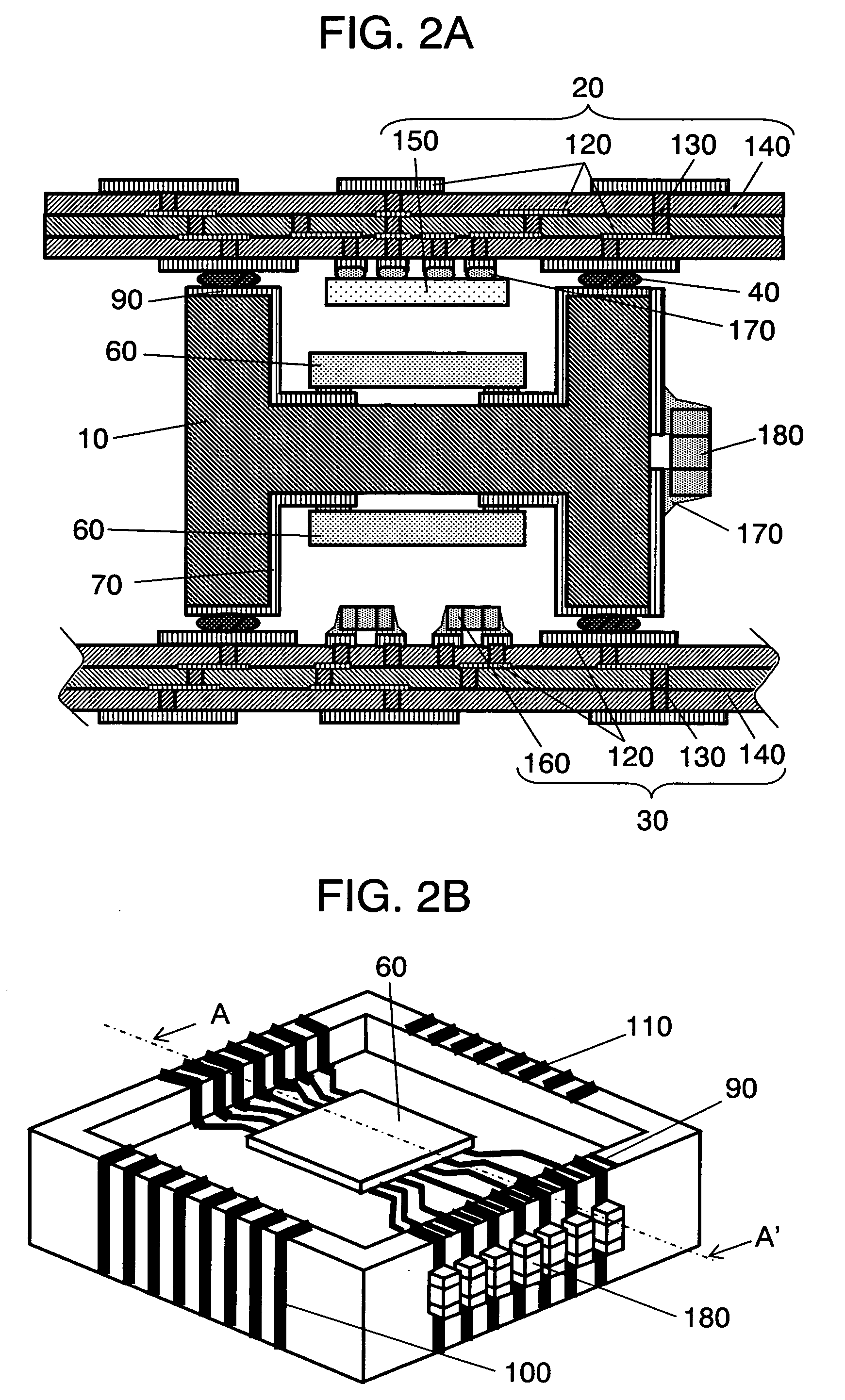
[0098]FIGS. 5A and 5B show the structure of a stereoscopic electronic circuit device according to a second embodiment of the present invention. FIG. 5A is a cross sectional view taken along the line A-A′ of FIG. 5B, and FIG. 5B is a perspective view of relay board 10 shown in FIG. 5A.

[0099] Similar to that of the first embodiment, this stereoscopic electronic circuit device has a three-dimensional connection structure in which first circuit board 20 and second circuit board 30 are connected with each other electrically and mechanically via relay board 10 disposed therebetween by using connection members 40.

[0100] As shown in FIG. 5B, relay board 10 has recesses 50. Recesses 50 are mounted with electronic components 60 and are provided with lead-out wirings 70 extending from electronic components 60. Relay board 10 also has land parts 90 which are connected with lead-out wirings 70, and which connect between lead-out wirings 70 and first circuit board 20 or second circuit board 30 ...

third embodiment

[0112]FIGS. 11A and 11B show the structure of a stereoscopic electronic circuit device according to a third embodiment of the present invention. FIG. 11A is a cross sectional view taken along the line A-A′ of FIG. 11B, and FIG. 11B is a perspective view of relay board 260 shown in FIG. 11A.

[0113] In FIG. 11A, relay board 260 has, on its side surface other than opposed surfaces 80, recess 290 on which to mount electronic component 60. The side surface is provided with lead-out wirings 70 extending from electronic component 60, and with board interconnections 100 for connecting first circuit board 20 and second circuit board 30. Opposing surfaces 80 of relay board 260 are provided with land parts 90 to be connected to lead-out wirings 70, and also provided with board connection lands 110 to be connected to board interconnections 100. Relay board 26 has another side surface having another recess 300 formed thereon which is mounted with electronic component 310 and which is molded usin...


PUM


Abstract

A stereoscopically connected structure is made up of a first circuit board and a second circuit board which are mounted with other electronic components, and a relay board having a recess which is mounted with an electronic component and is provided with a lead-out wiring extending from the electronic component, and also having a land part to be connected with the lead-out wiring on one of the surfaces of the relay board that face the first circuit board and second circuit board. Thus the relay board can mount the electronic component thereon as well as connect the first circuit board and the second circuit board, thereby achieving high density mounting.

Description

BACKGROUND OF THE INVENTION [0001] 1. Field of the Invention [0002] The present invention relates to a stereoscopic electronic circuit device in which circuit boards mounted with electronic components are connected stereoscopically with each other by using a relay board or the like, and also relates to a shield structure thereof. [0003] 2. Background Art [0004] In recent years, as electronic devices have been reduced in size and weight, there has been a strong demand for improving mounting density in electronic circuit devices having resistors, capacitors, semiconductor elements and the like mounted on an insulating circuit board. In addition, as electronic devices have been operated at higher speed and frequency, there have been rigorous demands for satisfying the criteria of EMC (Electromagnetic Compatibility) which indicates the ability to avoid malfunction due to external electromagnetic waves or not to interfere with the operation of other electronic devices. [0005] Conventiona...

Claims


Application Information

Patent Timeline
IPC IPC(8): H01L23/538H01L25/065H05K1/00H05K1/14H05K1/18H05K3/34H05K3/36H05K3/40
CPCH01L23/5385H01L2924/15192H01L2225/06572H01L2924/09701H05K1/0284H05K1/141H05K1/144H05K1/145H05K1/183H05K3/3442H05K3/368H05K3/403H05K2201/09036H05K2201/10446H05K2201/10636H05K2201/10674H05K2203/1572H01L2223/6677H01L2224/16225H01L2924/3025H01L2224/48091H01L2224/48227H01L2224/73265H01L2924/15156H01L25/0652H01L2924/1627H01L2924/181Y02P70/50H01L2924/00012
Inventor ONO, MASAHIROKONDO, SHIGERUNISHIKAWA, KAZUHIROYAGI, YOSHIHIKONISHIDA, KAZUTO
Owner PANASONIC CORP
Why Eureka
Try Eureka