Optical modulator and optical modulator array

an optical modulator and array technology, applied in the field of optical modulators and optical modulators, can solve the problems of low production yield, low production yield, and generally non-robust devices, and achieve the effects of high degree of freedom in design, excellent robustness, and easy production

Inactive Publication Date: 2005-08-11
FUJIFILM BUSINESS INNOVATION CORP
View PDF4 Cites 26 Cited by
  • Summary
  • Abstract
  • Description
  • Claims
  • Application Information

AI Technical Summary

Benefits of technology

[0017] The present invention has been accomplished in order to solve the above-described problems, and provides an optical modulator and an optical modulator array, which are easily produced, have excellent robustness, and have a novel structure which allows high degree of freedom in design and highly controlled modulation of light intensity.
[0022] The optical modulator and the optical modulator array of the invention are effective in that they are easily produced and have excellent robustness, as well as they allow high degree of freedom in design and highly controlled modulation of intensity of light.

Problems solved by technology

Therefore, they usually require a relatively large voltage to be applied on the optical crystal.
Although the Mach-Zehnder Modulators are widely used for the above-described reasons, fabrication conditions for these devices are quite severe, resulting in low production yield.
However, branching ratios of such optical directional couplers are very sensitive to materials (for example, refractive indices) and production conditions (for example, degrees of channel separations), which make these devices generally non-robust.
Therefore, the multi-mode interferometer device provides no advantage, other than enabling the even splitting of an optical power, over conventional Mach-Zehnder Modulators.
As described above, the currently widely used Mach-Zehnder Modulators, which use a Y-branch waveguide and / or an optical directional coupler, are not capable of evenly splitting an optical power, and have a problem that it is difficult to produce highly precise optical modulators with a high production yield.
However, in such optical modulators, the multi-mode interferometer device is used merely as a passive device, and therefore, no optical modulator has been existed, in which the multi-mode interferometer device is employed as an active device involved in phase modulation.

Method used


Image

  • Optical modulator and optical modulator array
  • Optical modulator and optical modulator array
  • Optical modulator and optical modulator array

Examples


Embodiment Construction

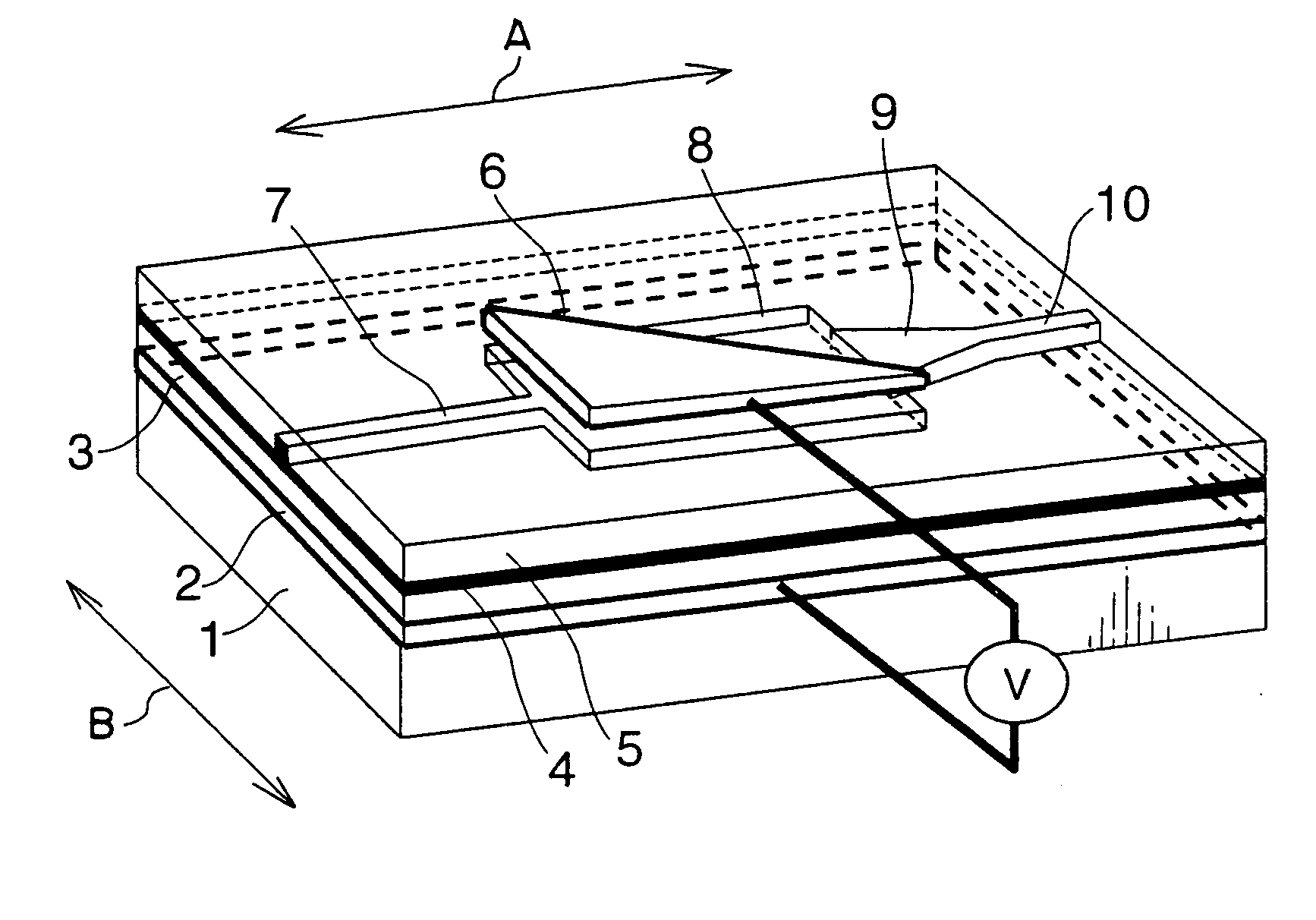
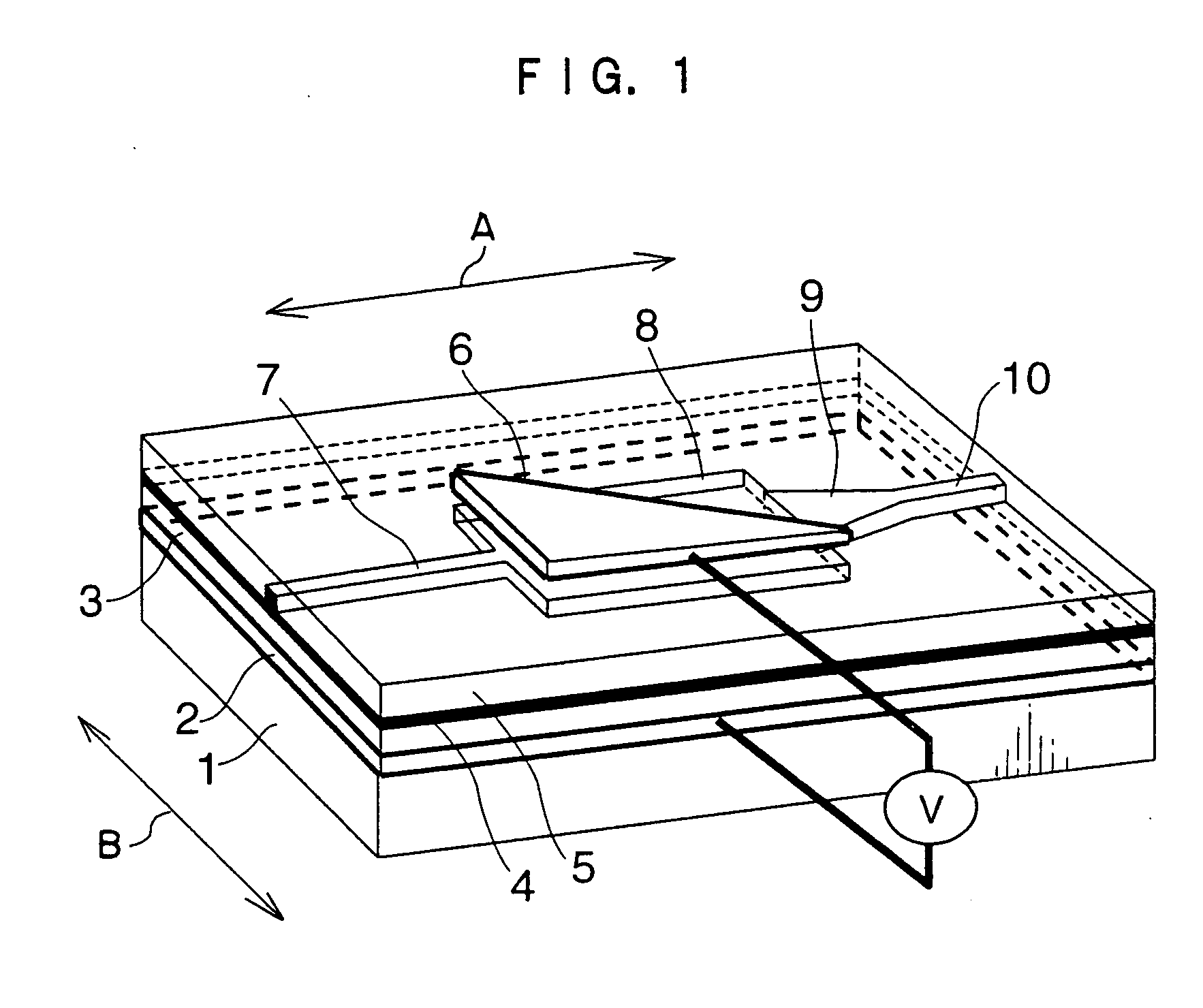
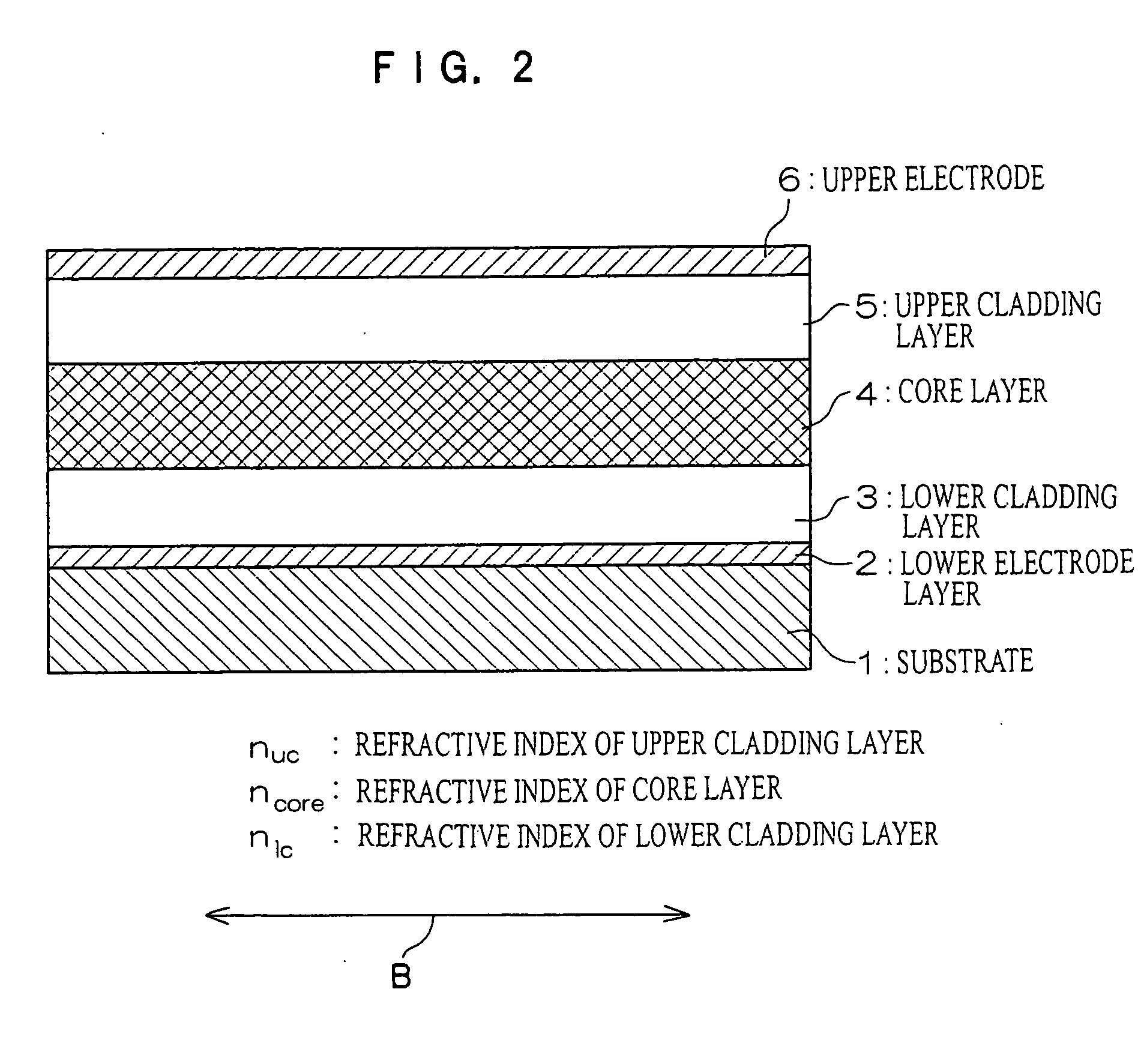
[0038] As shown in FIGS. 1 and 2, an optical modulator according to this embodiment includes a substrate 1, a lower electrode layer 2 laminated on the substrate 1, a lower cladding layer 3 laminated on the lower electrode layer 2, a core layer 4 laminated on the lower cladding layer 3, an upper cladding layer 5 laminated on the core layer 4, and an upper electrode 6 laminated on the upper cladding layer 5.

[0039] Where a refractive index of the lower cladding layer 3 is nlc, a refractive index of the core layer 4 is ncore, and a refractive index of the upper cladding layer 5 is nuc, values of the refractive indexes have to be set to satisfy the following conditions, respectively:

ncore>nlc

ncore>nuc, and

nlc=nuc or nlc≠nuc.

[0040] An optical waveguide is disposed in the core layer 4. The optical waveguide is formed by an input-side single-mode waveguide 7, a wide multi-mode waveguide 8, a tapered waveguide 9 and an output-side single-mode waveguide 10. The input-side single-mode wav...


PUM

PropertyMeasurementUnit
thicknessaaaaaaaaaa
refractive indexaaaaaaaaaa
widthaaaaaaaaaa

Abstract

An optical modulator is provided with an optical waveguide including an input-side single-mode waveguide for propagating inputted light at single mode, a multi-mode waveguide for propagating the light propagated from the input-side single-mode waveguide at plural guided modes, and an output-side single-mode waveguide for propagating the light propagated from the multi-mode waveguide at single mode to output the light. A lower electrode layer is disposed below the multi-mode waveguide, and an upper electrode is disposed above the multi-mode waveguide. The upper electrode cooperates with the lower electrode layer to apply an electric field to the multi-mode waveguide. A phase of each of the guided modes propagating through the multi-mode waveguide is modulated by applying an electric field to the multi-mode waveguide, and intensity of the light outputted from the output-side single-mode waveguide is modulated by an interference of the phase-modulated guided modes.

Description

CROSS-REFERENCE TO RELATED APPLICATION [0001] This application claims priority under 35 USC 119 from Japanese Patent Application No. 2004-32575, the disclosure of which is incorporated by reference herein. BACKGROUND OF THE INVENTION [0002] 1. Field of the Invention [0003] The present invention relates to, an optical modulator and an optical modulator array. More particularly, the invention relates to an optical modulator and an optical modulator array that modulate an optical signal by utilizing interference between plural rays of guided mode light propagating through multi-mode interference waveguide. [0004] 2. Description of the Related Art [0005] Transmission systems that are capable of manipulating the phase and intensity of optical signals are very important. The most common devices among devices for modulating the phase and intensity of optical signals are optical modulators, which have rapidly become key devices. It should be noted that optical attenuators for attenuating th...

Claims


Application Information

Patent Timeline
Patent Type & Authority Applications(United States)
IPC IPC(8): G02F1/035G02B6/26G02B6/42G02F1/01G02F1/225
CPCG02F2001/217G02F1/225G02F1/217
Inventor THAPLIYA, ROSHANOKANO, YASUNORINAKAMURA, SHIGETOSHI
Owner FUJIFILM BUSINESS INNOVATION CORP
Why Eureka
Try Eureka