Electronic device and method of manufacturing the same

a technology of electronic devices and manufacturing methods, applied in the field of electronic devices, can solve the problems of molten al used as wiring for sensors, low diffusion velocity of hsub>2 /sub>to the exterior, and not expected to increase the vacuum level

Active Publication Date: 2005-08-11
PANASONIC CORP
View PDF11 Cites 76 Cited by
  • Summary
  • Abstract
  • Description
  • Claims
  • Application Information

AI Technical Summary

Benefits of technology

[0057] In a preferred embodiment, the production method further includes the step of, after the step (d) and bef...

Problems solved by technology

However, there exists a problem that an increase in vacuum level is not expected, for the purpose of improving the sensitivity of the sensor.
In the case where high temperature heating of 660° C. or more is performed, there arises a problem that Al used as wiring for the sensor is molten.
However, in such temperatures, the diffusion velocity of H2 to the exterior is very low, so that the function as the heating for increasing the vacuum level is not expected so much.
If the method described with reference to FIG. 12 is adopted in order to increase the vacuum level, it is extremely difficult to dispose the getter shown in FIG. 12 in the minute cavi...

Method used


Image

  • Electronic device and method of manufacturing the same
  • Electronic device and method of manufacturing the same
  • Electronic device and method of manufacturing the same

Examples


embodiment 1

[0179] Hereinafter a first embodiment of the present invention will be described with reference to the drawings.

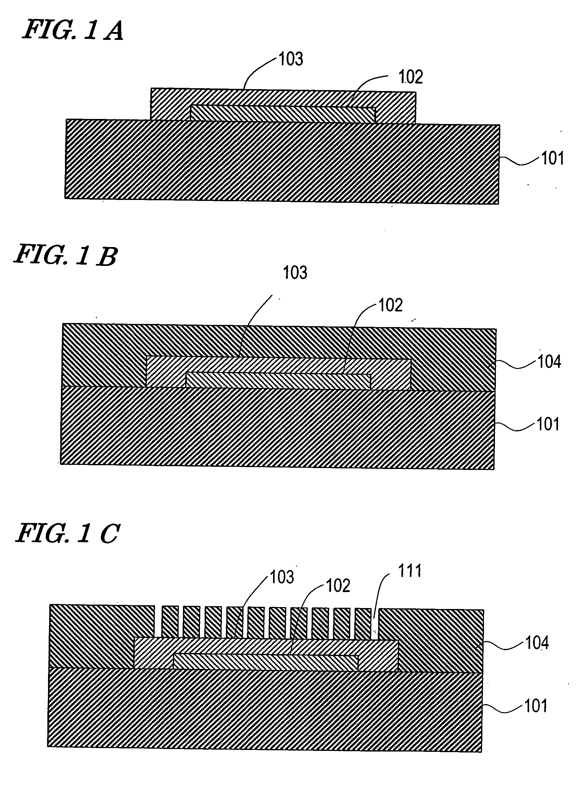
[0180] First, in a step shown in FIG. 4A, a detecting unit 12 such as a bolometer of an infrared sensor is formed on a main face of a silicon substrate 11. Specifically, after a thin film of a material having a sensor function is deposited on the silicon substrate 11, micro-fabrication such as photolithography and etching is performed, thereby patterning the thin film. A planar shape of the detecting unit 12 is designed so as to have the same planar shape as that of the resistive element 151 shown in FIG. 2, for example.

[0181] Next, after a silicon oxide film 13 which covers the detecting unit 12 is deposited on the silicon substrate 11 by a thin film deposition technique such as CVD, the silicon oxide film 13 is patterned so as to cover the detecting unit 12 and the peripheral portion thereof. The patterning can be also performed by photolithography and etching techniqu...

embodiment 2

[0197] Hereinafter a second embodiment according to the present invention will be described.

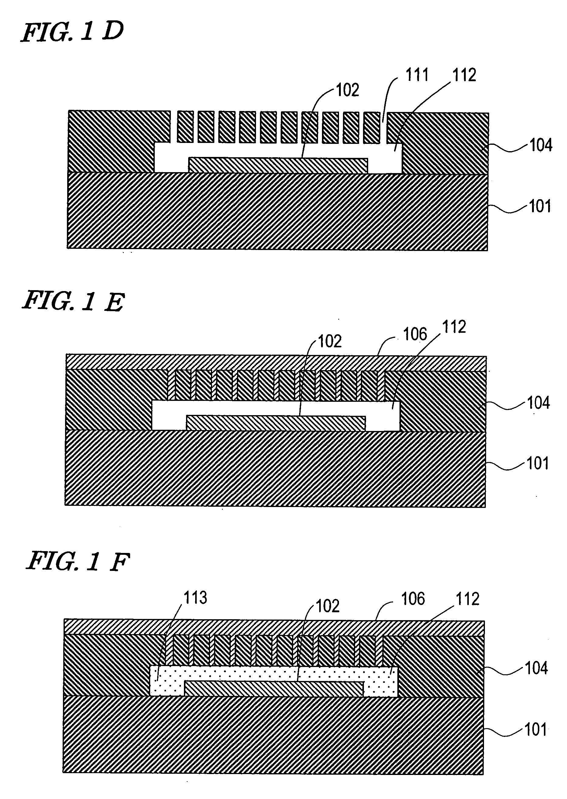
[0198] In the above-described first embodiment, the etching holes 21 are closed by the metal sealing member 16a by obliquely sputtering a metal from the above of the polysilicon film 14. Alternatively, instead of the oblique sputtering, if the shape of the etching hole 21 is contrived, the etching hole 21 can be closed by vertical sputtering.

[0199] FIGS. 5(a) and (b) are partial sectional views each showing part of a production process of an electronic device according to this embodiment. Both of FIGS. 5(a) and (b) show the configuration of the polysilicon film and the like formed in the step shown in FIG. 4E.

[0200] In the polysilicon film 14 of the electronic device according to a modification shown in FIG. 5(a), an etching hole 21a of a tapered shape is formed. In this modification, the sputtered metal is deposited on a tapered wall of the etching hole 21a, thereby closing the etching ho...

embodiment 3

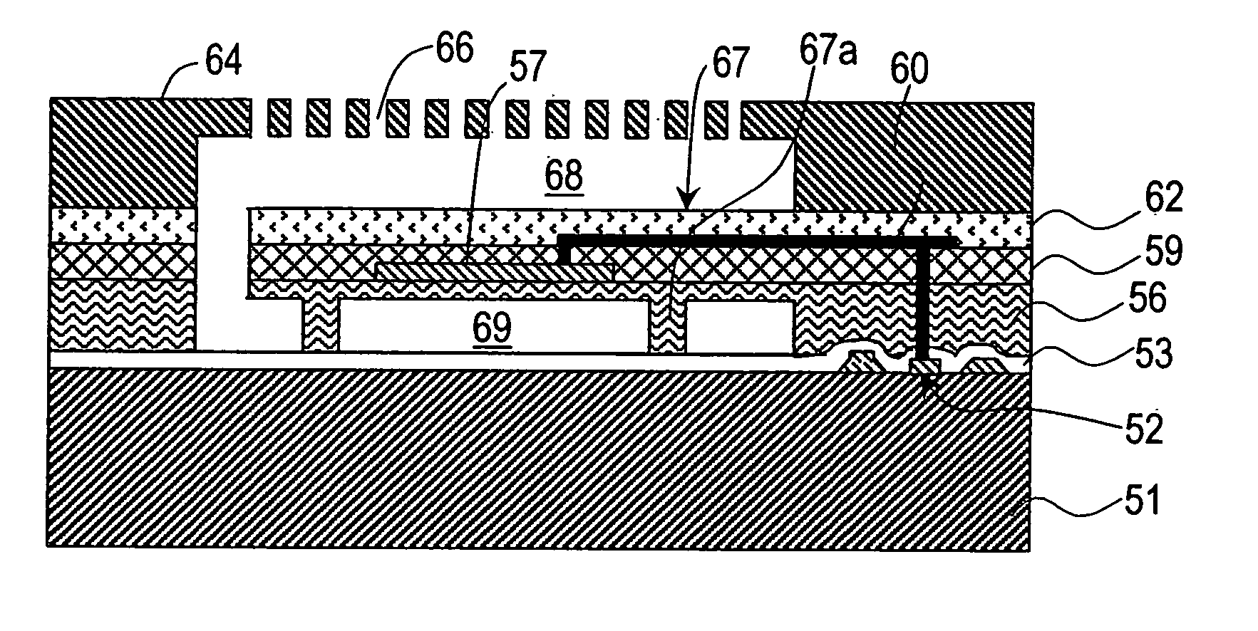
[0206] With reference to FIGS. 7A to 7N, a third embodiment according to the present invention will be described. FIGS. 7A to 7C are sectional views showing steps before a sacrificial layer is formed in a production process of an electronic device in this embodiment. FIGS. 7D to 7F are sectional views showing steps before a BPSG film is planarized after the sacrificial layer is formed in the production process of the electronic device according to this embodiment. FIGS. 7G to 7I are sectional views showing steps before a protection film and the like are patterned after the BPSG film is planarized in the production process of the electronic device according to this embodiment. FIGS. 7J to 7L are sectional views showing steps before etching holes are formed after the protecting film and the like are patterned in the production process of the electronic device according to the embodiment. FIGS. 7M and 7N are sectional views showing steps before a sealing member for closing the etching ...


PUM


Abstract

In the present invention, an etching hole 21 is formed in a polysilicon film 14 as a cavity-wall member. Through the etching hole 21, hydrofluoric acid is injected, so as to dissolve a silicon oxide film 13, thereby forming a cavity 22. In the cavity 22, a detecting unit 12 of a sensor is in an exposed condition. Next, by sputtering, an Al film 16 is deposited in the etching hole 21 and on an upper face of a substrate. Thereafter, a portion of the Al film 16 positioned on the polysilicon film 14 is removed by etching back, thereby leaving only a metal closure 16a of Al which closes the etching hole. The sputtering step is performed under a pressure of 5 Pa or less, so that the pressure in the cavity can be held to be low.

Description

TECHNICAL FIELD [0001] The present invention relates to an electronic device provided with a cavity of which an internal pressure is held at a low level and a production method thereof. The present invention particularly relates to an electronic device in which a sensing unit of an infrared sensor or the like is hermetically closed in an atmosphere of a reduced pressure, and a production method thereof. In addition, the present invention relates to an electronic device in which a pressure of the atmosphere in such a cavity can be measured, and the pressure can be further reduced as required, and a production method thereof. BACKGROUND ART [0002] For the purpose of increasing detection sensitivity, in an electronic device such as an infrared sensor, conventionally, at least a sensing unit is disposed in a cavity formed on a substrate, and the sensing unit is hermitically closed in a vacuum atmosphere or an inert gas atmosphere by a cap unit. [0003] Such electronic devices include, ot...

Claims


Application Information

Patent Timeline
IPC IPC(8): H01L27/14G01J1/02H01L35/32H01L35/34H01L37/00H01L37/02H04N5/33
CPCG01J5/045H01L37/02H01L37/00H10N15/00H10N15/10
Inventor IKUSHIMA, KIMIYAKOMOBUCHI, HIROYOSHIBABA, ASAKOUCHIDA, MIKIYA
Owner PANASONIC CORP
Why Eureka
Try Eureka