Spacer for a split gate flash memory cell and a memory cell employing the same

a memory cell and split-gate technology, applied in the field of split-gate flash memory cells and memory cells employing the same, can solve the problems of affecting the integrity of the memory cell, hindering the functionality and yield, and limited application, and achieves the effects of thinning composition, and reducing the over etching tim

Inactive Publication Date: 2005-08-11
TAIWAN SEMICON MFG CO LTD
View PDF8 Cites 11 Cited by
  • Summary
  • Abstract
  • Description
  • Claims
  • Application Information

AI Technical Summary

Benefits of technology

[0016] In one advantageous embodiment, the composite spacer forms a composite floating gate spacer proximate a floating gate of the split gate flash memory cell. In related aspects, the present invention provides a method of forming the composite spacer, and a split gate flash memory cell employing the same. By virtue of employing multiple materials with substantially opposite deposition distributions, the composite spacer achieves a more uniform construction notwithstanding a location of the split gate flash memory cell on the substrate.
[0017] In another aspect, the present invention provides another composite spacer for use with a split gate flash memory cell on a substrate. In one embodiment, the composite spacer includes a first spacer insulating layer having a substantially uniform deposition distribution across a surface thereof. The composite spacer also includes a second spacer insulating layer overlying the first spacer insulating layer and having a varying deposition distribution across a surface thereof. The second spacer insulating layer has a thinner composition in selected regions of the split gate flash memory cell thereby reducing an over etch time associated with an etching process to form the composite spacer.
[0018] In an advantageous embodiment, the composite spacer forms a composite contact spacer proximate a composite floating gate spacer of the split gate flash memory cell. In related aspects, the present invention provides a method of forming the composite spacer, and a split gate flash memory cell employing the same. Inasmuch as a layer of the composite spacer incorporates a varying deposition distribution across a surface thereof, an over etch time may be reduced in forming the composite spacer.
[0019] In yet another aspect, the present invention provides a coupling spacer for use with a split gate flash memory cell on a substrate having a substrate insulating layer thereon. In one embodiment, the coupling spacer includes a conductive layer that extends between a floating gate and the substrate insulating layer adjacent a source recessed into the substrate of the split gate flash memory cell thereby increasing a coupling area between the floating gate and the source. In related aspects, the present invention provides a method of forming the composite spacer, and a split gate flash memory cell employing the same. Inasmuch as the coupling spacer increases a coupling area between the source and floating gate, a coupling efficiency within the split gate flash memory cell is enhanced.

Problems solved by technology

While electrically erasable and programmable read only memory is electrically erasable and programmable per single byte, the application is limited due to the excessive footprint and attendant costs thereof.
The aforementioned split gate flash memory cell by Lin and other related memory cells suffer from design and fabrication limitations that hinder the functionality and yield thereof.
Additionally, over etching, if not kept in check, can deteriorate selected materials within the split gate flash memory cell thereby detracting from an integrity of the memory cell.
Inasmuch as the over etching window (i.e., the second opening 128) is very narrow, it is not practical to reduce an over etching time to remove the insulating material thereby subjecting the other materials within the split gate flash memory cell from being erroneously etched away.
Again, a low coupling efficiency between the floating gate and common source line may cause errors and, at the very least, inhibit the performance such as a programming speed of the split gate flash memory cell.
Accordingly, what is needed in the art is a split gate flash memory cell and related method of construction therefor that addresses the issues associated with non-uniform critical dimensions of the memory cells constructed across a substrate, over etching times within selecting regions of the memory cell, and low coupling efficiency between selected sections of the memory cell that overcomes the deficiencies in the prior art.

Method used


Image

  • Spacer for a split gate flash memory cell and a memory cell employing the same
  • Spacer for a split gate flash memory cell and a memory cell employing the same
  • Spacer for a split gate flash memory cell and a memory cell employing the same

Examples


Embodiment Construction

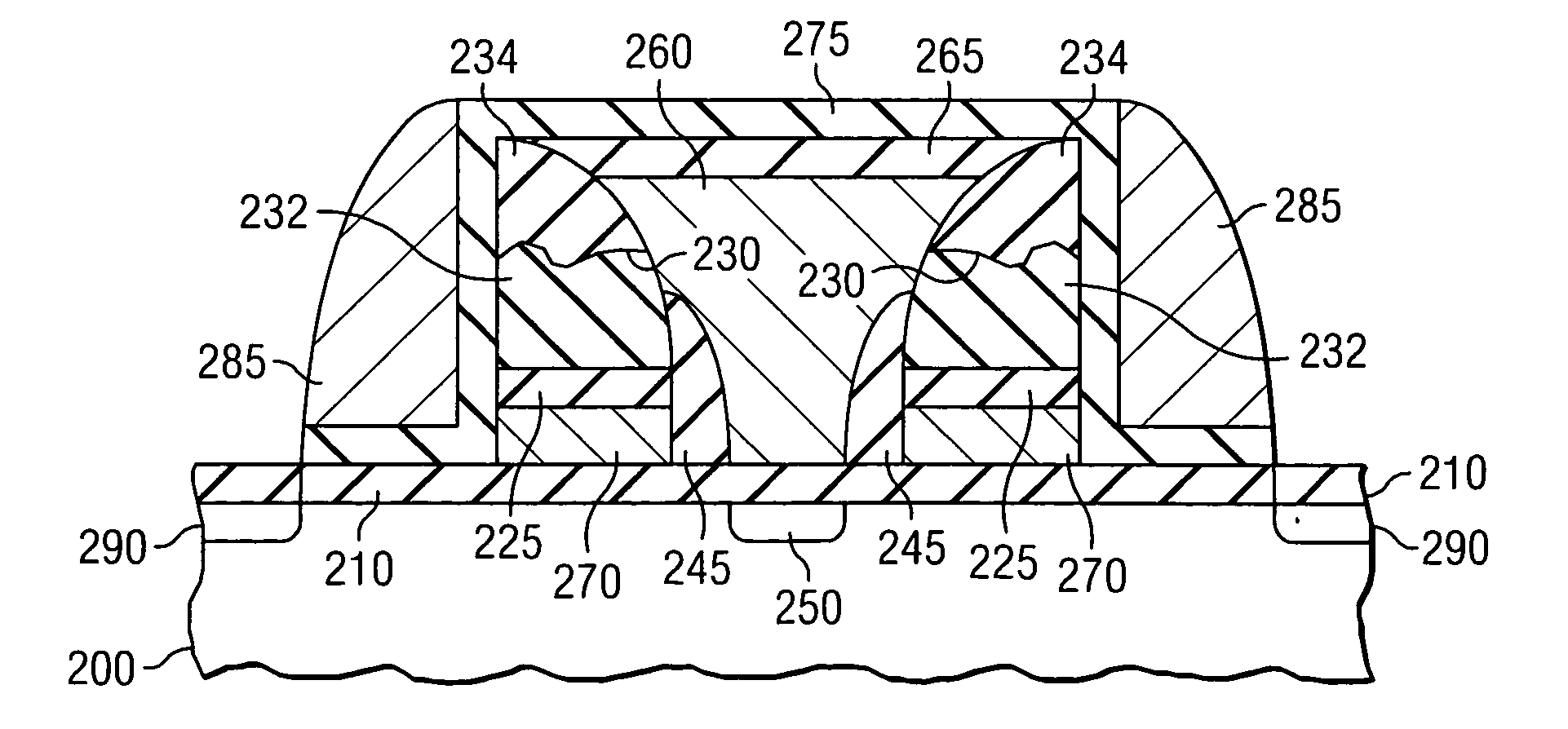
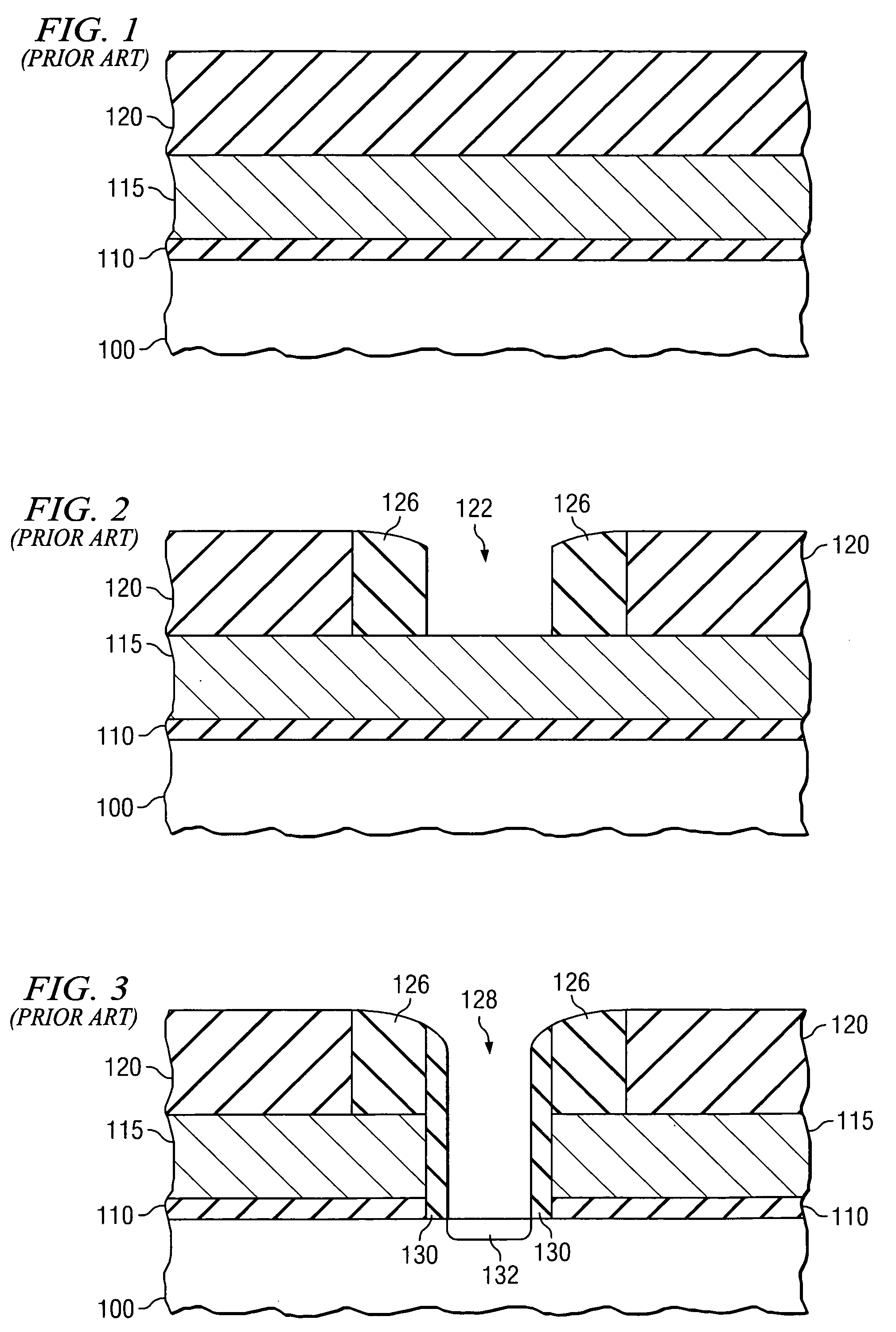
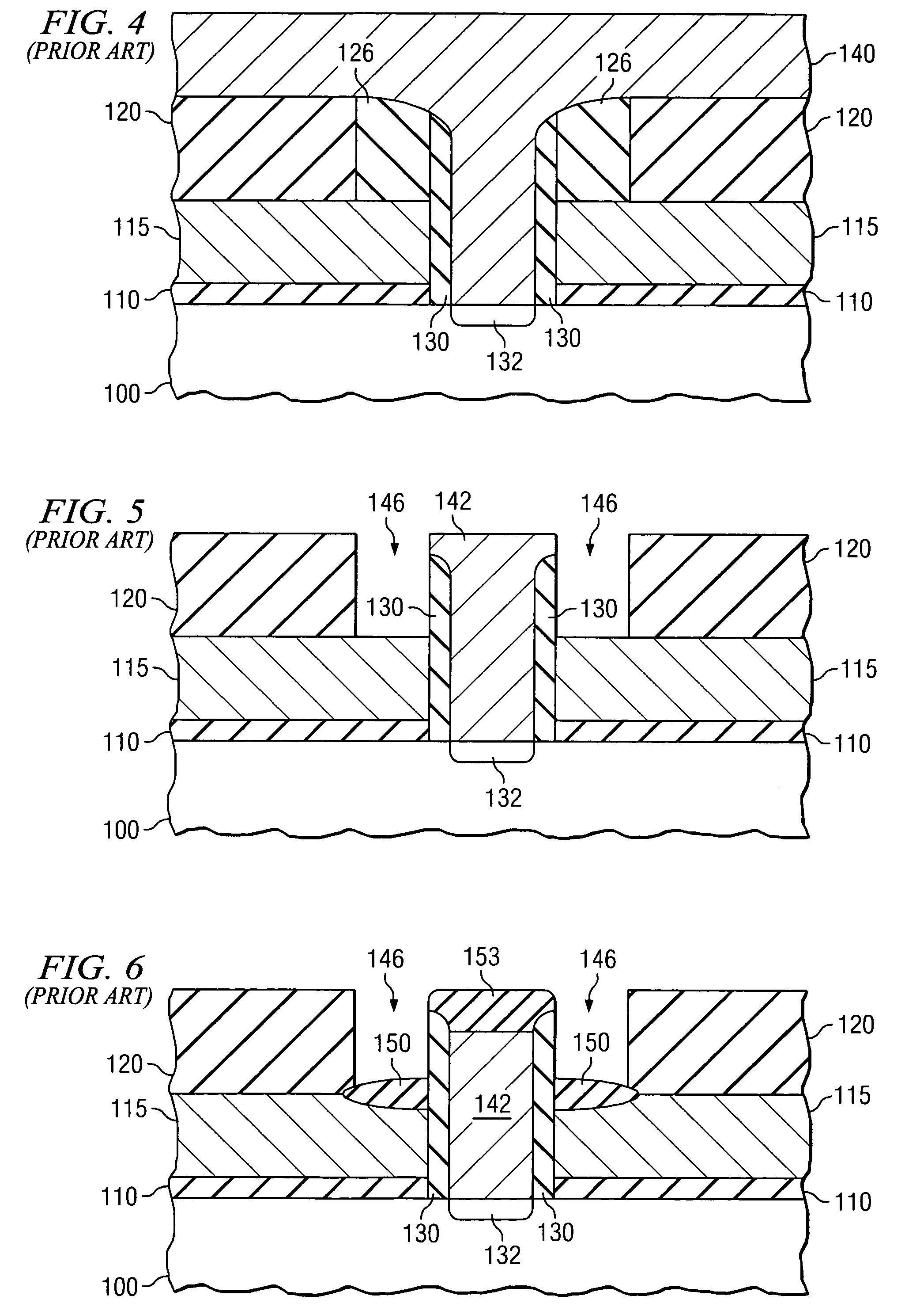
[0026] The making and using of the advantageous embodiments of a split gate flash memory cell are discussed in detail below. It should be appreciated, however, that the present invention provides many applicable inventive concepts that can be embodied in a wide variety of specific contexts. The specific embodiments discussed are merely illustrative of specific ways to make and use the invention, and do not limit the scope of the invention.

[0027] The present invention will be described with respect to advantageous embodiments in a specific context, namely, a spacer for a split gate flash memory cell, a split gate flash memory cell, and related method of forming the spacer and the split gate flash memory cell. The principles of the present invention, however, may also be applied to other semiconductor devices of like construction. The advantages associated with the split gate flash memory cell as disclosed herein further exploit the benefits associated with the application thereof.

[...


PUM


Abstract

A spacer, a split gate flash memory cell, and related method of forming the same. In one aspect, a composite spacer includes a first spacer insulating layer having a first deposition distribution that varies as a function of a location on a substrate. The composite spacer also includes a second spacer insulating layer having a second deposition distribution that varies in substantial opposition to the first deposition distribution. In another aspect, a composite spacer includes a first spacer insulating layer having a substantially uniform deposition distribution across a surface thereof. The composite spacer also includes a second spacer insulating layer having a varying deposition distribution with a thinner composition in selected regions of the memory cell. In another aspect, a coupling spacer provides for a conductive layer that extends between a floating gate and a substrate insulating layer adjacent a source recessed into the substrate of the memory cell.

Description

TECHNICAL FIELD [0001] The present invention is directed, in general, to semiconductor devices and, more specifically, to a spacer for a split gate flash memory cell, a split gate flash memory cell, and related method of forming the spacer and the split gate flash memory cell. BACKGROUND [0002] Complementary metal-oxide-semiconductor memory devices include random access memory and read only memory. The market share for read only memory has been continuously growing, especially in view of the development of flash memory in which a single cell can be electrically programmable and a block, sector or page of the cells may be simultaneously electrically erasable. Due to the electrically programmable but erasable characteristic of the flash memory, the market share of the flash memory as compared to electrically programmable read only memory has grown significantly. While electrically erasable and programmable read only memory is electrically erasable and programmable per single byte, the...

Claims


Application Information

Patent Timeline
Patent Type & Authority Applications(United States)
IPC IPC(8): H01L21/336H01L21/8246H01L21/8247H01L27/115H01L29/423
CPCH01L27/115H01L29/42324H01L27/11568H01L27/11521H10B69/00H10B41/30H10B43/30
Inventor LIU, YUAN-HUNGWU, CHIH-TATU, YEUR-LUENLO, CHI-HSINTSAI, CHIA-SHIUNG
Owner TAIWAN SEMICON MFG CO LTD
Why Eureka
Try Eureka