As the source / drain junction becomes shallower,
junction leakage caused by a
silicide (a compound of silicon and metal) becomes a problem.
However, by forming the sidewall to be thick, a problem arises in which resistivity increases at the junction part below the lower part of the sidewall (hereinafter referred to as the extension region).
However, because the silicon layer on the SOI surface is thin and the
silicide readily reaches to the BOX layer, an area between the silicide and the silicon shrinks significantly, creating another problem of increasing contact resistivity.
However, there is a problem in that the silicon single-crystalline film or the single crystalline film made of silicon-and-
germanium mixed crystal formed by vapor epitaxial growth tends to be influenced by impurities existing on the
substrate surface.
Therefore, when the impurities are found on the substrate, problems occur in which films cannot be formed by vapor epitaxial growth or the films grow as if interspersed with spots on the substrate.
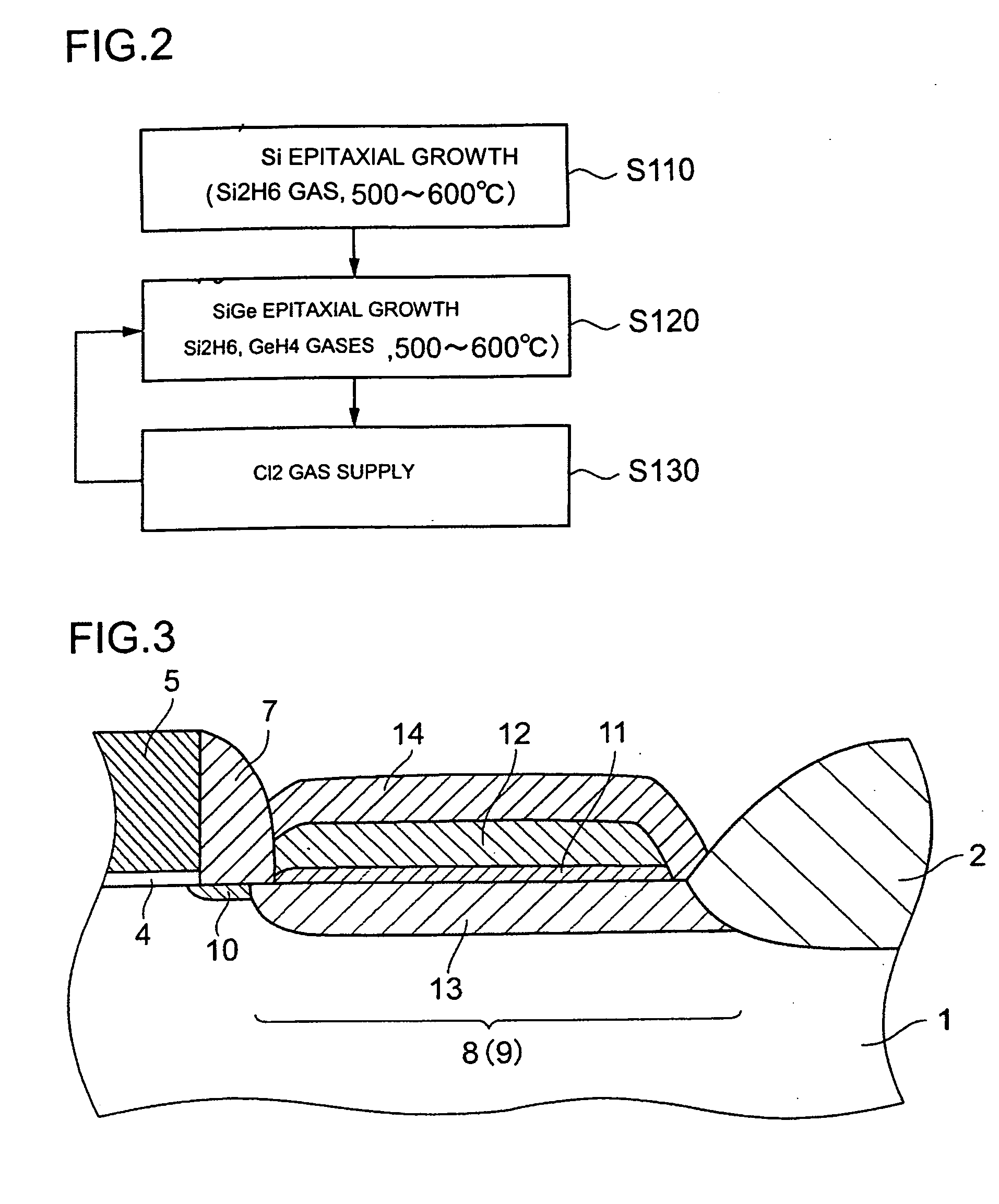
With the
processing temperature as low as 600° C. or less by the method according to Publication No. 10-125605, however, the substrate impurities cannot be removed, and, therefore, it is impossible to form a high-quality raised structure.
Moreover, at such low temperature, a problem arises in that the velocity at which the silicon single crystalline film is formed by vapor epitaxial growth decreases dramatically.
On the contrary, the silicon-and-
germanium mixed crystalline film has a relatively high film formation velocity; however, the silicon-and-germanium mixed crystalline film is largely influenced by the impurities on the substrate, and, therefore, the film formation process is not stable.
On the contrary, formation of a silicon buffer film is not easily influenced by the impurities on the
substrate surface.
Further, the reason for having the thickness of 10 nm or less is that, if it is very thick, there is a problem in which the
throughput of the film formation processes decreases since the velocity of vapor epitaxial growth of the silicon buffer film is low compared to that of the silicon-and-germanium mixed crystalline film.
Also, if a formed silicon-and-germanium mixed crystalline film is thicker than 100 nm, a problem of short circuiting tends to occur at the gate
electrode and the electrodes of the source part and the drain part.
Further, if it is thicker than necessary, other problems in the process occur, in which the film formation takes longer or the consumption of gas materials becomes larger.
Further, the reason for having the thickness of 10 nm or less is that, if it is very thick, there is a problem in which the
throughput of the film formation process decreases, since the velocity of vapor epitaxial growth of the silicon buffer film is low compared to that of the silicon-and-germanium mixed crystalline film.
Also, if the silicon-and-germanium mixed crystalline film is formed to have the thickness of 100 nm or more, a problem of short circuiting tends to occur at the gate electrode and the electrodes of the source part and the drain part.
Further, if the silicon-and-germanium mixed crystalline film is thicker than necessary, other problems in the process occur, in which the film formation process takes longer or the consumption of gas materials becomes larger.

