
Method of manufacturing crystalline film, method of manufacturing crystalline-film-layered substrate, method of manufacturing thermoelectric conversion element, and thermoelectric conversion element

a technology of crystalline film and manufacturing method, which is applied in the direction of thermoelectric device junction materials, thermoelectric device manufacturing/treatment, chemistry apparatus and processes, etc., can solve the problems of difficult to form a thermoelectric conversion layer thereon by epitaxial growth, difficult to peel off epitaxially grown crystalline film from a substrate,

Active Publication Date: 2005-08-18
PANASONIC CORP
View PDF1 Cites 34 Cited by
  • Summary
  • Abstract
  • Description
  • Claims
  • Application Information

AI Technical Summary

Benefits of technology

[0021] According to the methods of the present invention, an epitaxially grown crystalline film is made separable from a substrate by an action of water vapor on the layered structure. Unlike the separation that accompanies the removal of a substrate through plasma etching or the like, these methods do not cause damages to the thin film and moreover makes it possible to recycle the substrate used for growing the thin film. According to the present invention, a good quality crystalline film that is epitaxially grown can be obtained, and this crystalline film functions as a p-type thermoelectric conversion layer or an n-type thermoelectric conversion layer by appropriately selecting its composition.

Problems solved by technology

It is not easy to peel off an epitaxially grown crystalline film from a substrate; therefore, in practice, removal of the substrate by plasma etching or the like is necessary to separate the crystalline film from the substrate.
However, the removal of a substrate by plasma etching or the like tends to cause damages to the thin film and, moreover, makes it impossible to recycle the substrate.
However, since the materials of the soluble substrate or layer are limited, it is difficult to form a thermoelectric conversion layer thereon by epitaxial growth.
It is often the case that a substrate suitable for epitaxial growth does not match a substrate desirable when in use, not only for the thermoelectric conversion element but also for other functional elements.

Method used


Image

  • Method of manufacturing crystalline film, method of manufacturing crystalline-film-layered substrate, method of manufacturing thermoelectric conversion element, and thermoelectric conversion element
  • Method of manufacturing crystalline film, method of manufacturing crystalline-film-layered substrate, method of manufacturing thermoelectric conversion element, and thermoelectric conversion element
  • Method of manufacturing crystalline film, method of manufacturing crystalline-film-layered substrate, method of manufacturing thermoelectric conversion element, and thermoelectric conversion element

Examples


example 1

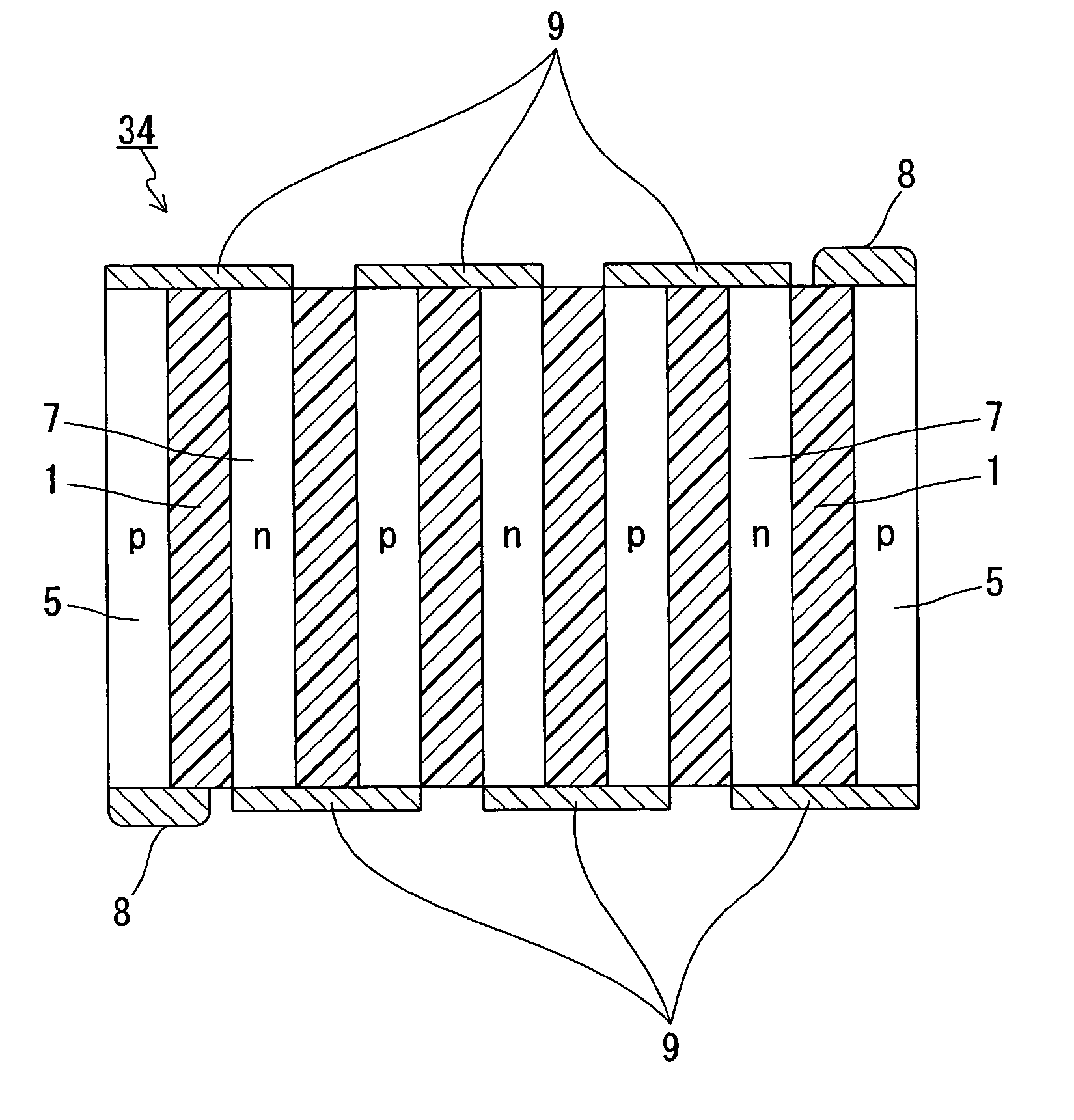
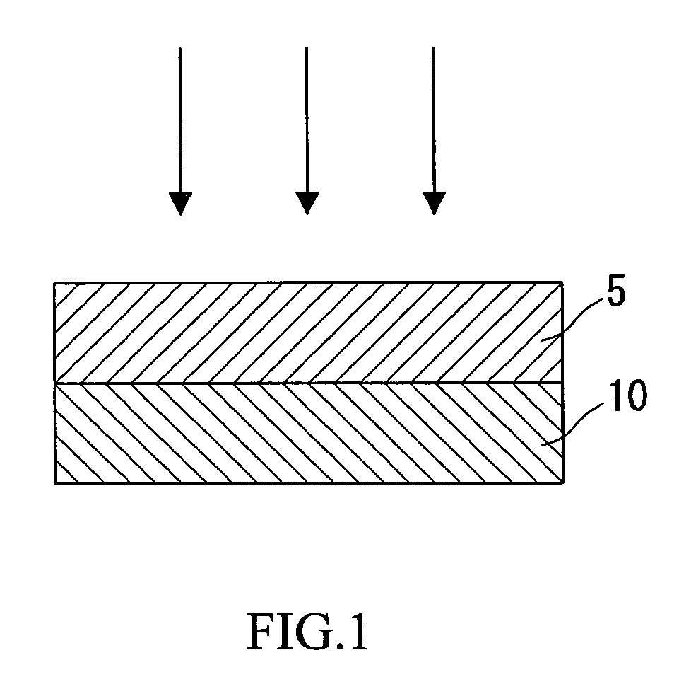
[0075] A p-type thermoelectric conversion layer 5 represented by the formula Na0.5CoO2 was epitaxially grown on a single-crystal sapphire substrate 10 by sputtering, and an n-type thermoelectric conversion layer 7 represented by the formula Na0.5(Ti0.8Cu0.2)O2 was epitaxially grown on another single-crystal sapphire substrate 10. The sputtering was carried out using targets that were weighed to have the compositions of the above respective formulae and were mixed to be uniform under an atmosphere of Ar gas and O2 gas being mixed at 3:1 at a pressure of 5 Pa, with the substrate temperature being kept at 700° C. By the sputtering for about 2 hours, the thickness of both of the thermoelectric conversion layers became about 900 nm.

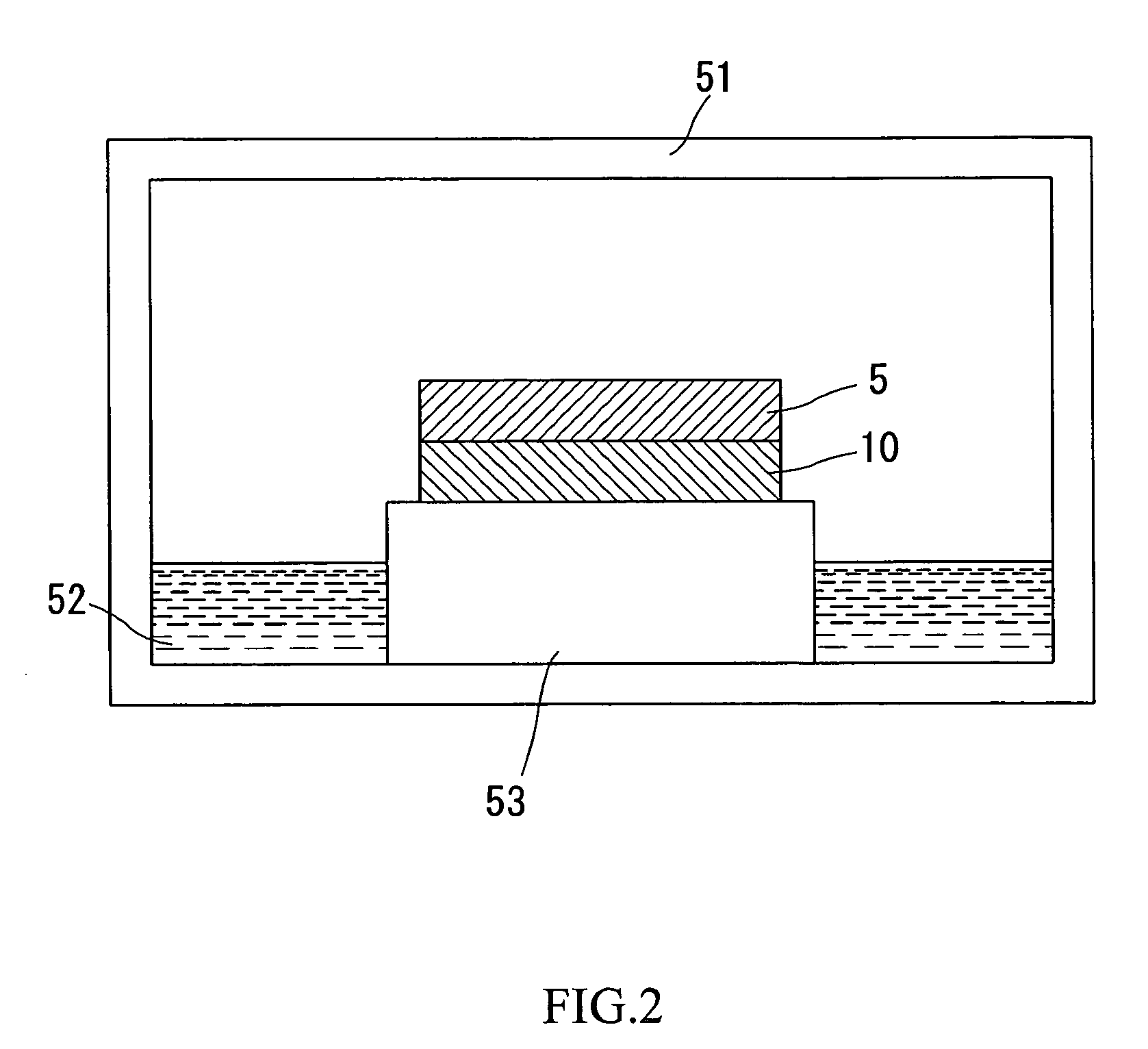
[0076] The two substrates 10 thus obtained were placed into a chamber in which water was accommodated as in FIG. 2 and were set aside for 3 hours in a constant temperature bath at 70° C. Thereafter, a 0.1 mm-thick acrylic plate 1 was pressed against the surfa...

example 2

[0079] Peltier-type thermoelectric conversion elements 37 and 38 were fabricated in the same manner as in Example 1 except that a double layer film of a film represented by the formula Na0.5CoO2 and a ZnO film doped with Al at 2% was formed as the n-type thermoelectric conversion layer 7 in place of Na0.5(Ti0.8Cu0.2)O2. For the n-type thermoelectric conversion layer, a film represented by the formula Na0.5CoO2 was epitaxially grown to a thickness of 50 nm, and thereafter, on the resulting film, a c-axis oriented ZnO film doped with Al was grown to a thickness of 900 nm.

[0080] In place of the Al-doped ZnO film, it was also possible to epitaxially grow a film represented by the formula (Sr0.9La0.1)TiO3 on the film represented by the formula Na0.5CoO2. This film was epitaxially grown along a (111) plane.

[0081] In the case where Na0.5(Ti0.8Cu0.2)O2 was used in place of Na0.5CoO2 as the film having a layered structure as well, it was possible to epitaxially grow an Al-doped ZnO film.


PUM

PropertyMeasurementUnit
thicknessaaaaaaaaaa
thicknessaaaaaaaaaa
temperatureaaaaaaaaaa

Abstract

It is often the case that a substrate suitable for epitaxial growth does not match a substrate desirable for the use in functional elements such as thermoelectric conversion elements or the like. The present invention makes it possible to separate a predetermined layered structure formed on a substrate therefrom through an action of water vapor. A method of manufacturing a crystalline film of the present invention includes the steps of: epitaxially growing on a substrate a crystalline film including a layered structure so that the layered structure comes into contact with the substrate; contacting water vapor supplied from a water vapor source with the layered structure in a chamber; and separating the layered structure that has been contacted with the water vapor from the substrate to obtain the crystalline film. The layered structure has a layer containing an alkali metal, and a layer containing an oxide of at least one element selected from the group consisting of Co, Fe, Ni, Mn, Ti, Cr, V, Nb, and Mo.

Description

BACKGROUND OF THE INVENTION [0001] 1. Field of the Invention [0002] The present invention relates to a method of manufacturing a crystalline film and a crystalline-film-layered substrate, and to a method of manufacturing a thermoelectric conversion element using the foregoing method. The present invention also relates to a thermoelectric conversion element including a crystalline film obtained by epitaxial growth as a thermoelectric conversion layer. [0003] 2. Description of the the Related Art [0004] Thermoelectric power generation is a technology for directly converting thermal energy into electric energy with the use of the Seebeck effect, a phenomenon in which a temperature difference given to opposing ends of a substance causes a thermal electromotive force in proportion to the temperature difference. The thermal electromotive force can be taken out as electric power by connecting a load thereto and forming a closed circuit. This technology has been in practical use as power su...

Claims


Application Information

Patent Timeline
Patent Type & Authority Applications(United States)
IPC IPC(8): H10N10/01H10N10/17H10N10/85H10N10/855H10N15/00
CPCH01L35/22H01L35/34H01L35/32Y10S117/915H10N10/855H10N10/01H10N10/17
Inventor YOTSUHASHI, SATOSHIADACHI, HIDEAKISUGITA, YASUNARIKANNO, TSUTOMU
Owner PANASONIC CORP
Learn More