Electronic imaging system

a technology of electronic imaging and image sensor array, which is applied in the field of imaging system, can solve the problems of inability to achieve the correct exposure of a dark scene, the radiation intensity of light the single white led element is too low to achieve the effect of correct exposure, and the effect of high electric power saving efficiency

Inactive Publication Date: 2005-08-18
FUJI PHOTO OPTICAL CO LTD
View PDF4 Cites 79 Cited by
  • Summary
  • Abstract
  • Description
  • Claims
  • Application Information

AI Technical Summary

Benefits of technology

[0010] It is therefore an object of the present invention to provide an electronic imaging system equipped with an image sensor device having a sequential exposure rolling shutter that enables a lighting unit comprising LED elements to produce flashes at a high emission efficiency and a high electric power saving efficiency.
[0012] According to the imaging system thus configured, since the LED array is kept flashing for a period of time between initiation of charge integration of the first row of the image sensor array and termination of charge integration of the last row of the image sensor array, flashes can affect charge integration of all the rows of the image sensor array even at high shutter speeds under which charge integration of all the rows do not overlap one another. Furthermore, the LED array can flash at a higher emission efficiency and a higher electric power saving efficiency as compared with the conventional imaging system which causes the LED element to flash in advance through operation of the first button and then makes exposure through operation of the second button after fixing composition of the image.

Problems solved by technology

One of the problems that the imaging system equipped with a rolling shutter encounters is that, although flashes can be enabled to affect charge integration (exposure) of all the rows of the image sensor array that overlap one another for a certain period of time when the shutter speed is low as shown in FIG. 11A, a flash is only allowed to affect charge integration (exposure) of some adjacent pixel rows of the image sensor array when the shutter speed is high as shown in FIG. 11B, because it is impossible for the image sensor array that all the rows have periods of charge integration overlapping one another.
However, the lighting unit comprising a single white LED element has the problem that light the single white LED element emits is too low in radiation intensity to make correct exposure in a dark scene.
However, this simultaneous excitation of white LEDs causes another problem that electric power consumption increases according to the number of excited white LEDs.
In particular, in the case where the single white LED is installed in cellular phone having an optical communication feature in addition to the image import feature, even if the white LED can have radiation intensity, the cellular phone will be disabled to make calls or data communication due to a potential drop of batteries resulting from image import and is off from practical use.
Further, there is no suggestion in the referenced publications how to coordinate sequential exposure by the rolling shutter and lighting control of the LED together.

Method used


Image

  • Electronic imaging system
  • Electronic imaging system
  • Electronic imaging system

Examples


Embodiment Construction

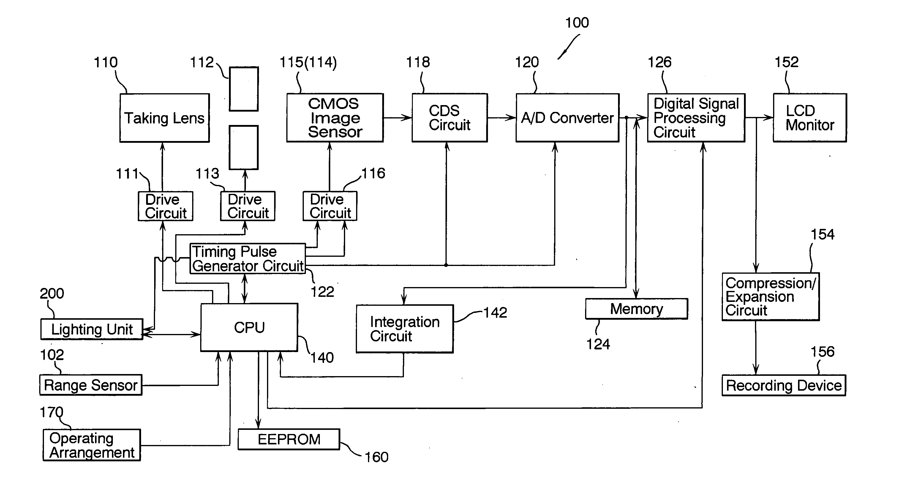
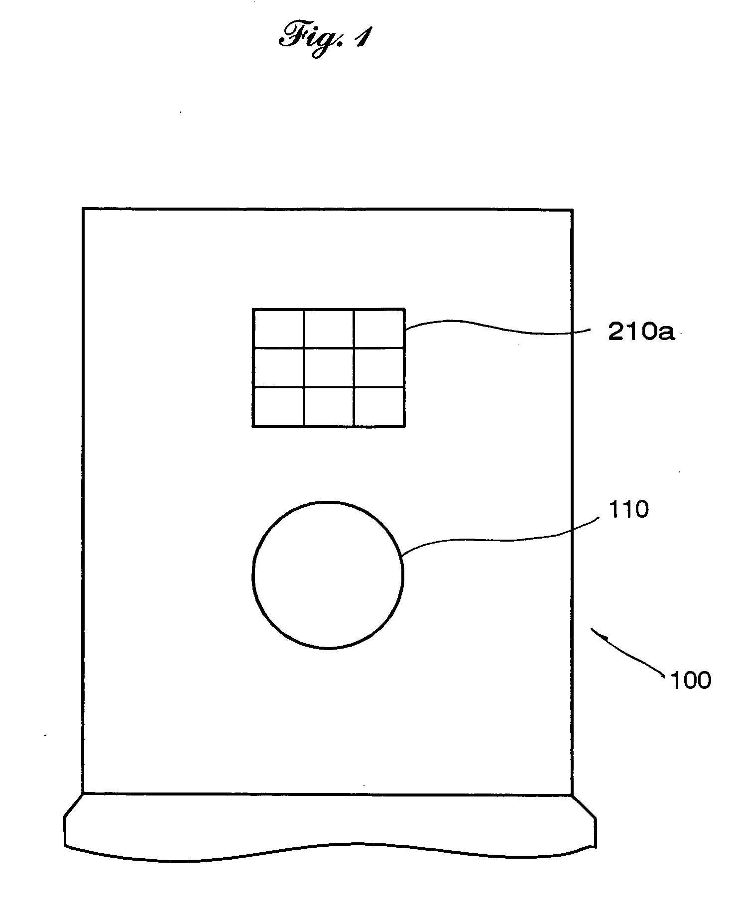
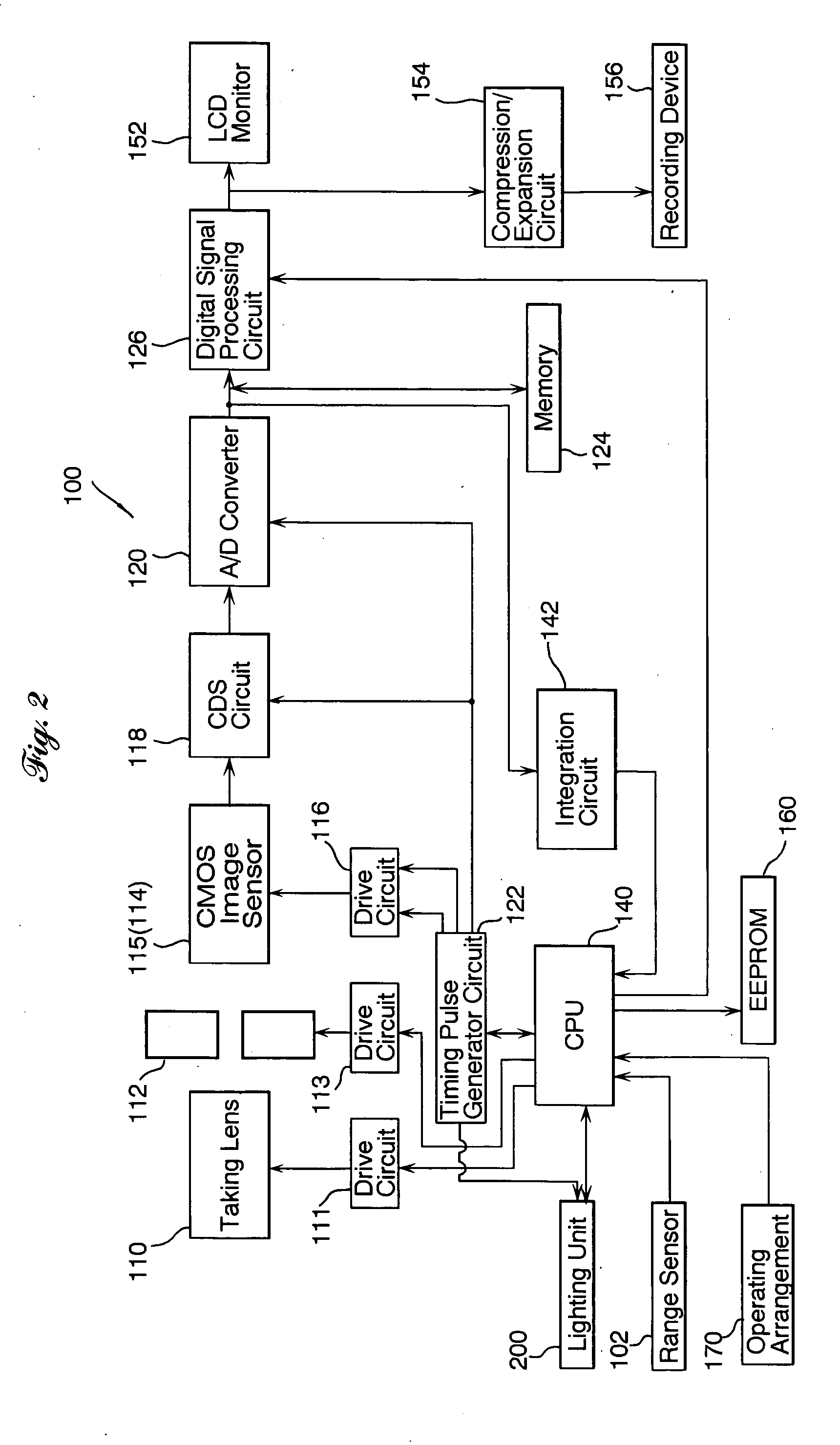
[0026] Referring to the accompanying drawings in detail, and in particular, to FIG. 1 schematically showing an electronic imaging system 100, such as a digital still camera, according to an embodiment of the present invention, the imaging system 100 includes a taking lens 110, specifically a zoom lens in this embodiment, and a lighting unit 200 comprising an array of light emitting diodes (which is hereinafter referred to as an LED array) 210a for producing subsidiary flashes which is installed at a side that faces an aimed subject in a scene to be captured. The LED array 210a comprises a number of white LED elements arranged in a plurality of roes. These white LED elements have lighting axes different from one another so as to produce flashes toward different areas of a scene covered by a field of view of the zoom lens 110, respectively. All of the incident light falling on the scene which includes available light indoor illumination light, other ambient light and flashes from the ...


PUM


Abstract

An electronic imaging system having an image sensor array that includes photodetectors arranged in rows and a rolling shutter for initiating charge integration by row and reading out pixel signals by row after a lapse of a predetermined integration time is equipped with a lighting unit having an LED array including rows of LED elements for producing flashes in different directions, respectively, and a circuitry for exciting and extinguishing the LED rows, one at a time. The LED rows are allocated to a plurality of sections into which the image sensor array is divided, one row to each section. The circuitry initiates excitation of each LED row allocated to a given section of the array at the beginning of charge integration of a first row of the given section and extinguishes the LED row at termination of charge integration of a last row of the given section.

Description

BACKGROUND OF THE INVENTION [0001] 1. Field of the Invention [0002] The present invention relates to an imaging system and, more specifically, to an electronic imaging system equipped with a sequential exposure rolling shutter. [0003] 2. Description of Related Art [0004] In recent years, it is a noticeable trend to employ complementary metal-oxide semiconductor (CMOS) image sensor devices for electronically capturing images of subjects in electronic imaging systems in light of the advantages of low cost, small size and low electric power consumption. Such a CMOS image sensor device generally comprises an image sensor array of photodetectors, one for each pixel, arranged in two-dimensional and a rolling electronic shutter or circuitry, in place of a mechanical shutter, for readout of the pixel signals. The photodetector for each pixel in the image sensor array converts photons impinging on the pixel to an electric charge via the photoelectric effect. The charge is integrated over a p...

Claims


Application Information

Patent Timeline
Patent Type & Authority Applications(United States)
IPC IPC(8): H01L27/00H04N5/238H04N5/235
CPCH04N5/2354H04N5/374H04N5/3532H04N23/74H04N25/531H04N25/76
Inventor YOSHIDA
Owner FUJI PHOTO OPTICAL CO LTD
Why Eureka
Try Eureka