ESD protection structure with lower maximum voltage

a protection structure and maximum voltage technology, applied in the direction of semiconductor devices, semiconductor/solid-state device details, electrical apparatus, etc., can solve the problems of certain maximum doping of the base, breakdown of the integrated circuit, and the destruction of the integrated circui

Inactive Publication Date: 2005-08-18
INFINEON TECH AG
View PDF5 Cites 0 Cited by
  • Summary
  • Abstract
  • Description
  • Claims
  • Application Information

AI Technical Summary

Benefits of technology

[0011] It is the object of the present invention to provide an improved ESD protection structure that can be sized such that its breakdown voltage is higher than a required operating voltage and its voltage drop in the ESD case is below a damaging effect for the integrated circuit.
[0016] Thereby, a symmetrical construction of the semiconductor structure is provided, which leads to a particularly favorable breakdown behavior in the ESD case and effects a space-saving construction.
[0018] It is also advantageous when there is a space between the third area and the second protective zone and between the second area and the second protective zone, respectively. Thereby, it is to be prevented that the protective zone has a negative effect on the space charge region at the pn junction between the third and second area, respectively, and the well.
[0020] It is advantageous when the second dopant concentration is higher than the first dopant concentration. Thereby, the well can be used as base for a bipolar transistor.
[0021] Preferably, the third, fourth and fifth dopant concentration are higher than the second dopant concentration. Contact zones—particularly emitter and collector of a bipolar transistor are formed by the higher third and fourth dopant concentration, while the conductivity of the protective zone is higher than the conductivity of the well due to the higher fifth dopant concentration, which leads to a lowering of the resistance in the well as a whole. Thus, in the ESD case, less voltage drops across the semiconductor structure. Thus, a damage to the integrated circuit to be protected is avoided.

Problems solved by technology

This can possibly lead to the destruction of the integrated circuit.
A voltage drop, which is too high, could lead to breakdowns of the integrated circuit.
Thus, a certain maximum doping of the base cannot be exceeded.

Method used


Image

  • ESD protection structure with lower maximum voltage
  • ESD protection structure with lower maximum voltage
  • ESD protection structure with lower maximum voltage

Examples


Embodiment Construction

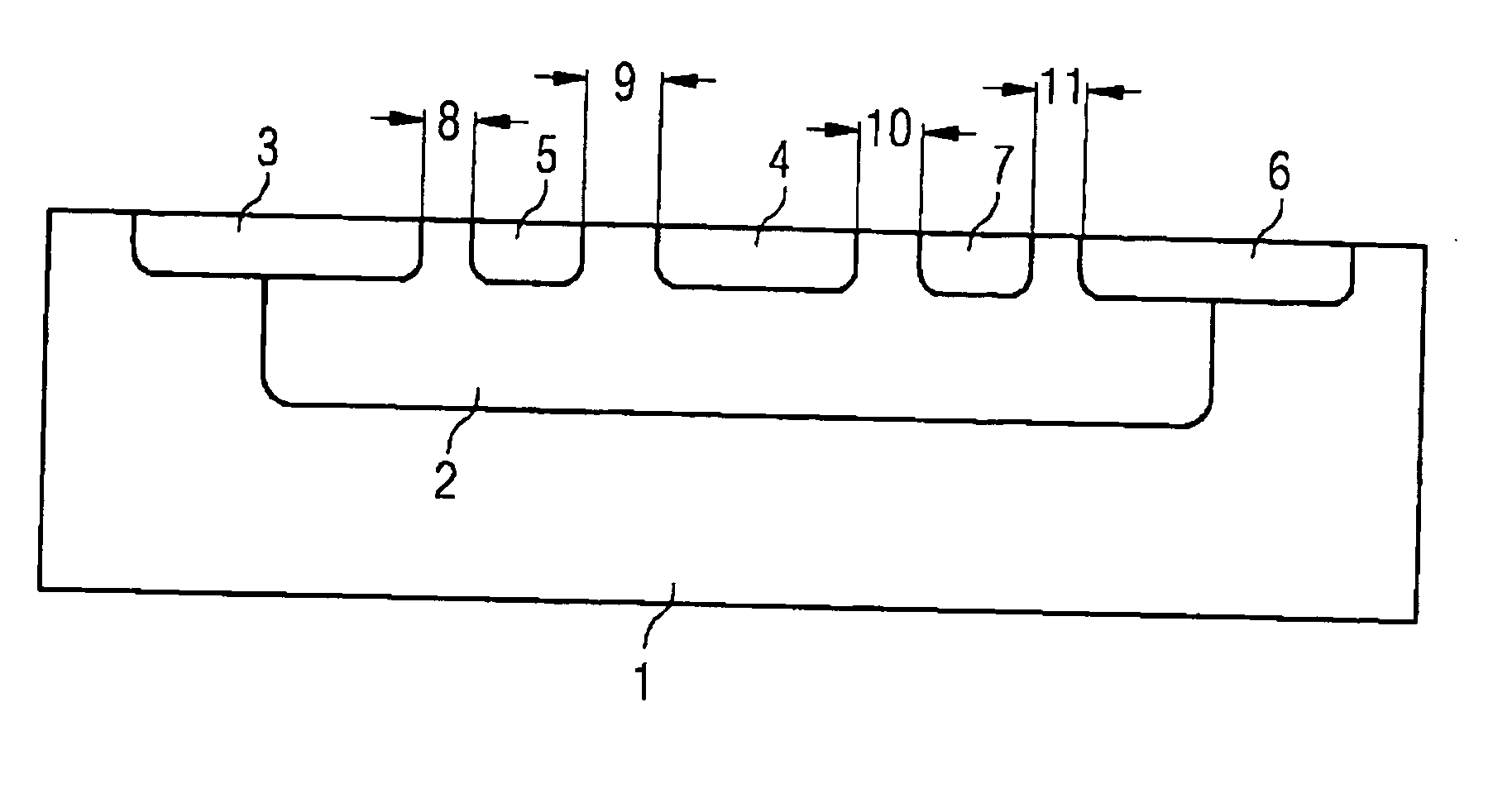
[0029] A preferred embodiment of the inventive semiconductor structure is illustrated in FIG. 1 in a schematical cross section view. A well 2 with an n dopant concentration of maximum 5×1017 cm−3 lies in a p semiconductor substrate with a p dopant concentration of about 1×1015 cm−3. The well 2 is implanted into the semiconductor structure 1 with a phosphor dose of about 4.5×1013 cm−2 and extends from a surface of the semiconductor substrate 1 about 4 to 5 μm into the center of the semiconductor substrate 1. The well 2 serves as base for a pnp bipolar transistor.

[0030] A first area 3 is at the first side edge of the well 2. The first area 3 extends also from the surface of the semiconductor substrate into its center. Thereby, a first part of the first area 3 is within the well 2, while a second part is outside the well 2 in the semiconductor substrate 1. Thus, in a later application, the first area 3 can be connected to ground potential.

[0031] The first area 3 is p doped with a max...


PUM


Abstract

A semiconductor structure for protecting integrated circuits from ESD pulses includes a semiconductor substrate of a first conductivity type and with a first dopant concentration. A well of a second conductivity type and with a second dopant concentration lies within the semiconductor substrate. Additionally, the semiconductor structure comprises a first area of a first conductivity type and with a third dopant concentration, wherein at least a first part of the area lies within the well. Further, there is a second area of a first conductivity type and with a fourth dopant concentration, the second area being fully within the well. A first protective zone of a second conductivity type and with a fifth dopant concentration lies in the well between the first area and the second area.

Description

BACKGROUND OF THE INVENTION CROSS-REFERENCE TO RELATED APPLICATION [0001] This application claims priority from German Patent Application No. 102004007972.2, which was filed on Feb. 18, 2004 and is incorporated herein by reference in its entirety. [0002] 1. Field of the Invention [0003] The present invention relates to a semiconductor structure for the protection of integrated circuits from ESD pulses. [0004] 2. Description of the Related Art [0005] If electrically charged subjects or persons are brought into contact with an input or output of an integrated circuit, a discharge can take place, where a current exceeding the standard measure flows through to the integrated circuit and a high voltage drops across the same. This can possibly lead to the destruction of the integrated circuit. [0006] For the protection of integrated circuits from these electrical discharges, so called ESD pulses (ESD=electrostatic discharge) the inputs and outputs of the integrated circuits are provided w...

Claims


Application Information

Patent Timeline
Patent Type & Authority Applications(United States)
IPC IPC(8): H01L23/62H01L27/02H01L27/082H01L31/072
CPCH01L27/0259
Inventor TADDIKEN, HANS
Owner INFINEON TECH AG
Why Eureka
Try Eureka