Substrate having a light emitter and image display device

Inactive Publication Date: 2005-08-18
CANON KK
View PDF7 Cites 32 Cited by
  • Summary
  • Abstract
  • Description
  • Claims
  • Application Information

AI Technical Summary

Benefits of technology

[0064] (2) The resistance Rz is such that the voltage drop is not substantially generated by the current injected from the electron-emitting device for the purpose of the image display.
[0065] With reference to (1), although the resistance Rz depends on the accelerating voltage applied to the image display device or the size of the display area, it is preferable that an effect of the current restriction is exhibited when the resistance Rz is more than 500Ω, and it is more preferable that the resistance is not lower than 5 KΩ. With reference to (2), although the resistance Rz depends on the amount of current injected from the electron-emitting device, the voltage drop caused by the current injected from the electron-emitting device becomes sufficiently small when the resistance Rz is lower than 1 MΩ, and more preferably the voltage drop can substantially be neglected when the resistance Rz is not more than 100 KΩ.
[0066] With reference to (1), when the resistance Rx is lower than 1 KΩ, the current flowing through the resistance Rx becomes large. Therefore, although the resistance Rx depends on the accelerating voltage applied to the image display device or the size of the display area, the resistance Rx is set to not lower than 1 KΩ to exhibit a current restriction. More preferably, the resistance Rx is set to 1 MΩ or more, for practical use.
[0067] For the method of connecting each conductive film 15 and the conductive area 12 or the high-voltage power supply 16 by-the resistance described above, the method in which the connection is performed not through the opening member 17 according to the invention but through the conductive fluorescent material may be used. However, almost all of the fluorescent materials which emit the light by the electron beam irradiation are the insulating material, and light-emission color and light-emission efficiency are sacrificed whe

Problems solved by technology

However, there are the following problems in the flat panel display in which

Method used


Image

  • Substrate having a light emitter and image display device
  • Substrate having a light emitter and image display device
  • Substrate having a light emitter and image display device

Examples


example 1

[0083] The image display device including the display panel shown in FIGS. 1A and 4 was produced.

[0084] In Example 1, the distance between the rear plate 21 and the faceplate 10 was set to 2 mm. The inside of the sealed vessel formed by the rear plate 21, the faceplate 10, and the sidewall 19 was maintained at a degree of pressure below 10−7 Pa. In Example 1, the number of row-direction electric line 22 was set to 240 (N=240), and the number of column-direction electric line 24 was set to 80 (M=80).

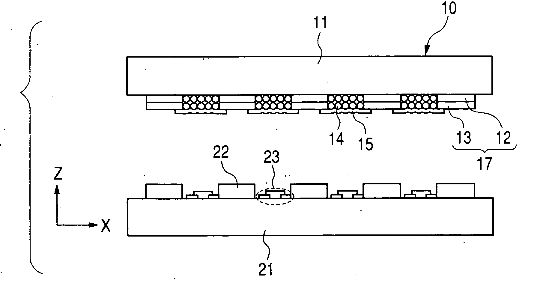
[0085]FIGS. 5A and 5B show the structure of the faceplate in Example 1. FIG. 5A is a schematic sectional view taken on dashed line of FIG. 5B, and FIG. 5B is a plan view when the faceplate is viewed from the rear plate side.

[0086] The process of manufacturing the faceplate of Example 1 will specifically be described below.

[0087] ITO which formed the conductive area 12 was deposited over the surface of the image area of the cleaned glass substrate by a sputtering method. A sheet resist...

example 2

[0096] The image display device including the display panel shown in FIG. 6A was produced. FIG. 6B is a plan view when the faceplate 10 is viewed from the side of the rear plate 21, FIG. 6A is a sectional view taken on line 6A-6A of FIG. 6B, and FIG. 6C is a sectional view taken on line 6C-6C of FIG. 6B.

[0097] In Example 2, the conductive area 12 was formed between the substrate 11 and the distance specifying member 13 while the pattern of the conductive area 12 was equal to that of the distance specifying member 13. Specifically, the conductive area 12 was formed so that the thickness of the paste containing the black pigments, silver particles, and the frit glass became 5 μm by the screen printing method using the glass substrate similar to Example 1. The subsequent processes were similar to Example 1 except that the thickness of the black matrix was set to 5 μm.

[0098] When the resistances Rx, Rz and Rp were measured in the same way as Example 1, Rx was 100 KΩ, Rz was 700Ω, and ...

example 3

[0101] The image display device including the display panel shown in FIG. 7A was produced. FIG. 7B is a plan view when the faceplate 10 is viewed from the side of the rear plate 21, FIG. 7A is a sectional view taken on line 7A-7A of FIG. 7B, and FIG. 7C is a sectional view taken on-line 7C-7C of FIG. 7B.

[0102] In Example 3, the conductive area 12 was formed in a line shape parallel to the Y-direction. Specifically, the conductive area 12 was formed so that the thickness of a photosensitive paste containing the black pigments, silver particles, and the frit glass became 2 μm by the screen printing method. Then, the dried photosensitive paste was exposed and developed to produce the plurality of line-shaped conductive areas 12 extending in the Y-direction. The subsequent processes were similar to Example 1 except that the thickness of the black matrix was set to 8 μm.

[0103] When the resistances Rx, Rz and Rp were measured in the same way as Example 1, Rx was 250 KΩ, Rz was 2 KΩ, and...


PUM


Abstract

An image display device which prevents damage to an electron-emitting device from discharge between a faceplate and a rear plate is provided. A conductive plate 12 including a transparent conductive film is formed over a surface of a substrate 1, a distance specifying member 13 having a plurality of openings is formed on the conductive area 12, a fluorescent material 14 is arranged in the opening, and a conductive film 15 is arranged on the fluorescent material 14 to for a face plate. A resistance Rx between the adjacent conductive films 15 is set larger than a resistance Rz, between the conductive film 15 and the conductive area 12. Discharge current generated between each conductive film 15 and a rear plate 21 is caused to flow into the conductive area 12 by applying anode voltage to the conductive area 12, which suppresses influence on an electron-emitting device 23.

Description

BACKGROUND OF THE INVENTION [0001] 1. Field of the Invention [0002] The present invention relates to a substrate having a light emitter which emits light by electron beam irradiation for an image display device, such as a field emission display, which utilizes an electron beam. The present invention also relates to an image display device using the substrate and an information display reproducing apparatus using the image display device. [0003] 2. Related Background Art [0004] Research and development of the image display device for which a field emission type electron-emitting device, a surface conduction electron-emitting device, and the like are used is in progress for a flat panel display of application. [0005]FIG. 13 shows an example of a display panel of the conventional image display device formed by using the surface conduction electron-emitting device. FIG. 13 is a perspective view schematically showing a structure while the display panel is partially cut off. In FIG. 13, t...

Claims


Application Information

Patent Timeline
IPC IPC(8): G09F9/30G09G3/10H01J1/62H01J29/32H01J29/08H01J29/28H01J29/46H01J31/12H01J31/15H01J63/04H01L31/12H05B33/14
CPCH01J29/085H01J2329/28H01J31/127H01J31/12H01J1/30
Inventor ONISHI, TOMOYA
Owner CANON KK
Why Eureka
Try Eureka