Liquid crystal display device, color filter substrate and protruding structure, and manufacturing method thereof

a liquid crystal display device and color filter substrate technology, applied in the field of display structure, can solve the problems of unwelcome features, partial uneven distribution of spacer density, and display image defects, and achieve the effects of reducing cost, simplifying fabrication process, and facilitating one-drop filling process

Active Publication Date: 2005-08-18
INNOLUX CORP
View PDF17 Cites 40 Cited by
  • Summary
  • Abstract
  • Description
  • Claims
  • Application Information

AI Technical Summary

Benefits of technology

[0017] According to various embodiments of the present invention, the spacers are directly disposed on the glass substrate, in which the spacers may have different heights. Hence when a pressure or force is applied on an LCD, the cell gap can be maintained. By utilizing the opening size of the masking pattern to adjust the depth of the exposure, protruding structures of different heights can be simultaneously formed, in which the protruding structures are able to serve as spacers or aligning protrusions to simplify the fabrication process and reduce cost. Moreover, the disclosed embodiments of the present invention facilitate a one drop fill process and further expands the operation window of the volume of dropped liquid crystals.

Problems solved by technology

In order to ensure proper operation of the LCD device, the cell gap has to be maintained precisely and uniformly, since imprecision within the cell gap can easily result in a defective display image (a condition usually referred to as mura).
Disposed randomly via a dispersion technique within the cell gap, the spacers 79 are equal in height, which often result in partial uneven distribution of the spacer density.
Additionally, the spacers are often disposed in both inactive and active areas of the display panel according to the conventional method.
In general, the structure and function of a LCD display utilized by the conventional spacer technique results in several unwelcoming features.
For instance, the spacers located within the active area will likely result in numerous disadvantages including reduced contrast or abnormal light irradiation in proximity to the edge of the spacers.
In other words, after a relatively large pressure is applied to the LCD panel, the uniformity of the cell gap will be disrupted, thereby resulting in effects such as mura.
When the number of spacers is too small or the elastic deformation is too large (such as a very small elastic coefficient), the volume of the liquid crystal is likely to overly increase, thereby resulting in gravity mura.
Conversely, when the number of spacers is too large or the elastic deformation is too small (such as a very large elastic coefficient), the volume of the liquid crystal will overly decrease, thereby generating air bubbles.

Method used


Image

  • Liquid crystal display device, color filter substrate and protruding structure, and manufacturing method thereof
  • Liquid crystal display device, color filter substrate and protruding structure, and manufacturing method thereof
  • Liquid crystal display device, color filter substrate and protruding structure, and manufacturing method thereof

Examples


Embodiment Construction

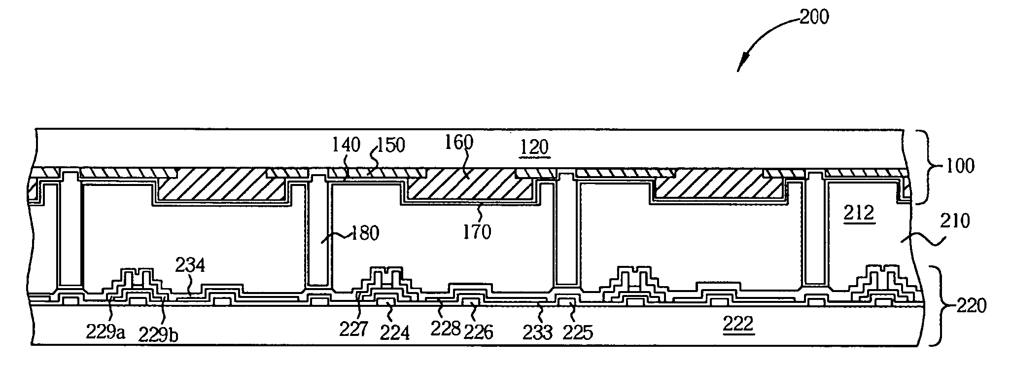
[0038] Please refer to FIGS. 4a, 4b, and 4c. FIGS. 4a, 4b, and 4c are perspective diagrams showing a spacer substrate according to some embodiments of the present invention. As shown in the figures, a color filter (CF) substrate 100 is utilized in a TFT LCD device.

[0039] As shown in FIG. 4a, a pixel of the CF substrate 100 includes three sub-pixels, in which the pixel is located corresponding to the thin film transistor of the TFT substrate (not shown). Please refer to FIGS. 4b and 4c. FIGS. 4b and 4c are cross-sectional diagrams showing the CF substrate 100 along the sectional line 4b-4b and 4c-4c. The CF substrate 100 includes a transparent substrate, such as a glass substrate 120, a black matrix 150 partially covering the glass substrate 120 for defining a plurality of pixel areas, in which the black matrix 150 is comprised of metals such as chromium (Cr) or chromium oxide (CrOx), or a black resin, and a spacer area 152.

[0040] Corresponding to inactive parts of the LCD device, ...


PUM

PropertyMeasurementUnit
heightaaaaaaaaaa
distanceaaaaaaaaaa
thicknessaaaaaaaaaa

Abstract

A liquid crystal display device, a color filter substrate and a protruding structure, and a manufacturing method thereof are provided. The color filter substrate includes a transparent substrate, a black matrix, a plurality of color filters, a plurality of first protruding structures, and a plurality of second protruding structures. The black matrix is disposed on the transparent substrate and exposes part of the transparent substrate for defining a plurality of first openings, a plurality of second openings, and a plurality of pixel regions, wherein the size of each first opening is different from the size of each second opening. In addition, the color filters are disposed in the pixel regions. The first protruding structures and the second protruding structures are disposed on the transparent substrate, wherein the first protruding structures correspond to the first openings respectively and the second protruding structures correspond to the second openings respectively.

Description

BACKGROUND OF INVENTION [0001] 1. Field of the Invention [0002] The present disclosure relates to a display structure and a method for fabricating the same, and more particularly, to the structure of a liquid crystal display device and a method for fabricating the same. [0003] 2. Description of the Prior Art [0004] A conventional liquid crystal display (LCD) device generally includes a pair of substrates, in which the substrates are parallel and separated from each other by a distance. The space between the substrates is usually referred to as the liquid crystal cell gap or, simply, cell gap. Additionally, a liquid crystal material is disposed between the two substrates within the cell gap, in which the liquid crystal material is able to respond to an outside electronic signal, thereby altering its optical characteristics. The electronic signal is controlled by a plurality of electrodes disposed on the inner surface of the substrates. The electrode arrangement of some particular LCD...

Claims


Application Information

Patent Timeline
Patent Type & Authority Applications(United States)
IPC IPC(8): G02F1/1333G02F1/1335G02F1/1337G02F1/1339
CPCG02F1/133512G02F2001/13415G02F1/13394G02F1/13415E02B7/005E02B7/205E02B7/54
Inventor CHEN, YU-JENWU, YUAN-LIANGLIN, CHING-SHAN
Owner INNOLUX CORP
Why Eureka
Try Eureka