
Inspection apparatus and method for film carrier tapes for mounting electronic components and semiconductor devices

a film carrier tape and inspection apparatus technology, applied in the direction of instruments, controlling lamination, transportation and packaging, etc., can solve the problems of inability to maintain the forward leaning position of the inspector, the inspector's microscopic foreign matter will more likely fall on the inspected film carrier tape, and the inspector's undue fatigu

Inactive Publication Date: 2005-08-25
MITSUI MINING & SMELTING CO LTD
View PDF5 Cites 6 Cited by
  • Summary
  • Abstract
  • Description
  • Claims
  • Application Information

AI Technical Summary

Benefits of technology

[0023] Accordingly, when two inspection apparatuses of the present invention are arranged with their back faces opposed to each other, both sides in the width direction of a pair of the inspection apparatuses can be used as passageways, permitting effective use of the space inside the inspection room.
[0044] The inspection apparatus of the invention is characterized in that it allows an inspector to conduct visual inspection of the film carrier tape at the inspection part in which the film carrier tape is transported in a vertical direction across the field of view of the inspector.
[0048] The inspection apparatus and method for film carrier tapes and semiconductor devices according to the present invention provide space-saving arrangement of the apparatuses by virtue of the compact apparatus size. Furthermore, the inspection apparatus and method enable the inspector to conduct visual inspection in a natural sitting position on a chair of appropriate height regardless of the magnification of the magnifier.

Problems solved by technology

Therefore, the inspector has to maintain the forward leaning position over a long time.
Further, microscopic foreign matters from the inspector will more likely fall on the inspected film carrier tape.
Because of this extended focal length, the inspector sitting on a chair of appropriate height is required to raise the seat height to conduct visual inspection through the eyepiece, which is unfavorable for safety reasons.
Because the visual inspection of the film carrier tape takes a long time as described above, such long inspection in a standing position causes undue fatigue to the inspector.

Method used


Image

  • Inspection apparatus and method for film carrier tapes for mounting electronic components and semiconductor devices
  • Inspection apparatus and method for film carrier tapes for mounting electronic components and semiconductor devices
  • Inspection apparatus and method for film carrier tapes for mounting electronic components and semiconductor devices

Examples


Embodiment Construction

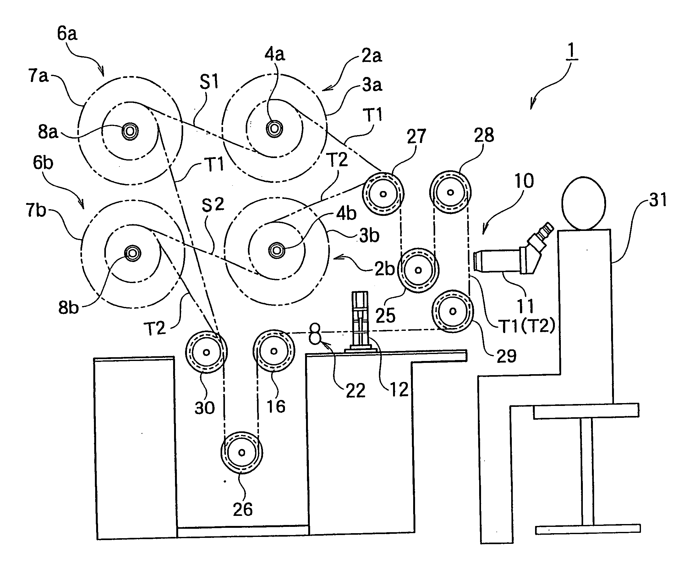
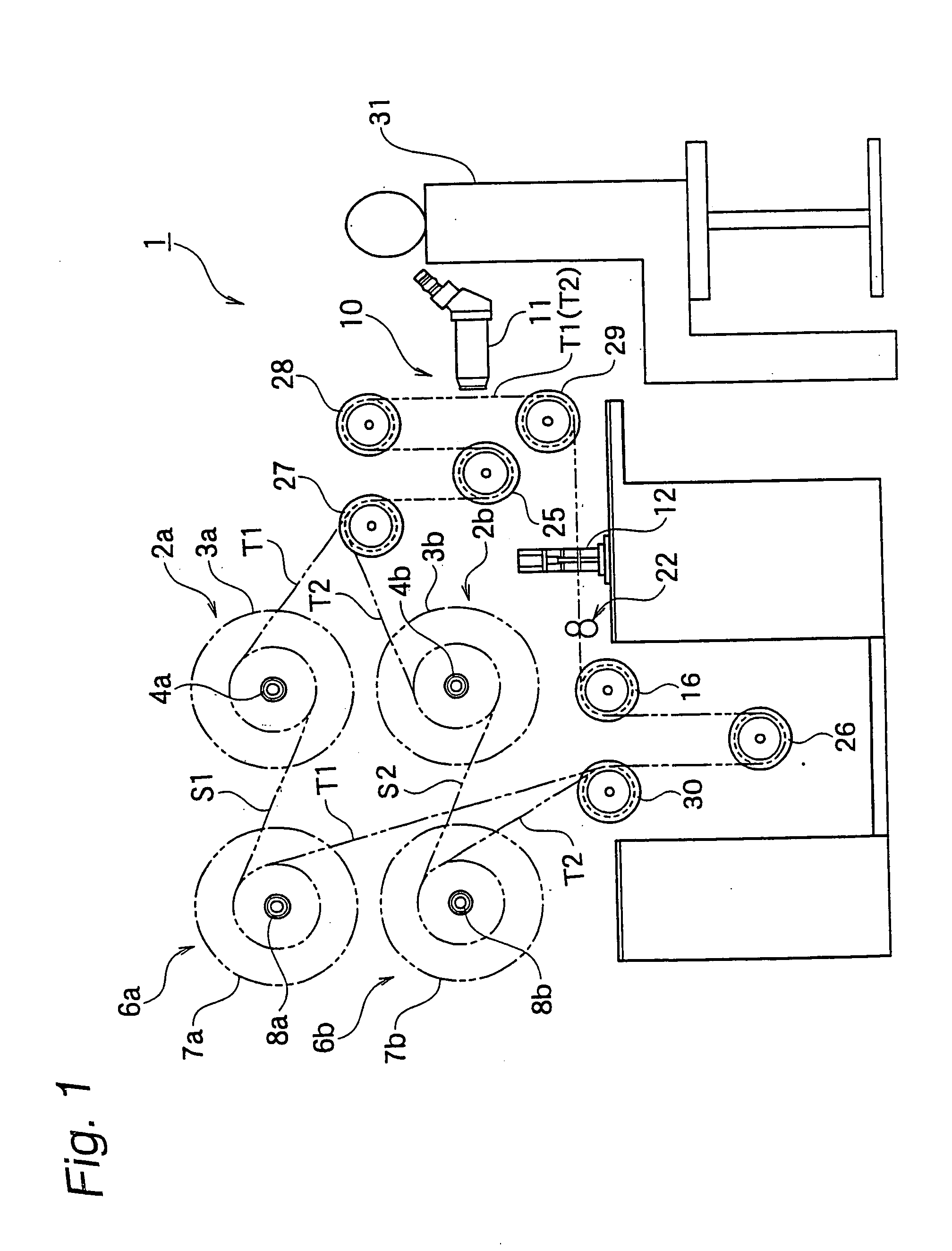
[0128] Hereinbelow, embodiments of the present invention will be described in detail with reference to the drawings. FIG. 1 is a front view illustrating the inspection apparatus for film carrier tapes according to an embodiment of the invention.

[0129] An inspection apparatus 1 for film carrier tapes illustrated in FIG. 1 (hereinafter, the inspection apparatus 1) is constituted to simultaneously inspect two film carrier tapes T1 and T2 for mounting electronic components (hereinafter, the film carrier tapes T1 and T2). The inspection apparatus is provided with feed devices 2a and 2b that feed the respective film carrier tapes T1 and T2, an inspection part 10, and take-up devices 6a and 6b that wind up the respective inspected film carrier tapes T1 and T2. The film carrier tapes T1 and T2 may be those obtained by, for example, cutting with a slitter a film carrier tape (so-called multiple-carrier tape) that is provided with a plurality of wiring pattern units including a part on which...


PUM

PropertyMeasurementUnit
Tensionaaaaaaaaaa

Abstract

An inspection apparatus and method of inspection enable an inspector to conduct visual inspection of film carrier tapes for mounting electronic components in a natural sitting position regardless of the magnification of a magnifier. The inspection apparatus is compact to permit effective use of the space inside the inspection room. The inspection apparatus includes a feed reel and a take-up reel adjacent to each other, and an inspection part that is located so that the adjacent feed and take-up reels are in the order of the feed reel and the take-up reel in relation to the inspection part. A film carrier tape from the feed reel is transported in a substantially vertical direction to the inspection part and is inspected with a magnifier along a substantially vertical direction.

Description

FIELD OF THE INVENTION [0001] The present invention relates to an apparatus and a method for inspecting film carrier tapes for mounting electronic components (hereinafter, the “film carrier tapes”) and semiconductor devices, wherein final inspection for defective leads and other defects is performed for the film carrier tapes before and after the mounting of semiconductors or other electronic components, and defective film carriers are marked as such by punching or the like. The inspection apparatus and method of the present invention may be suitably used for such film carrier tapes as TAB (tape automated bonding) tapes, COF (chip on film) tapes, T-BGA (tape ball grid array) tapes, CSP (chip size package) tapes, ASIC (application specific integrated circuit) tapes, and 2-metal (double-sided wiring) tapes. BACKGROUND OF THE INVENTION [0002] The demand for printed wiring boards for mounting electronic components such as IC (integrated circuits) tips and LSI (large-scale integrations) ...

Claims


Application Information

Patent Timeline
IPC IPC(8): B65B15/04C25D21/12G01N21/86G01N21/88H01L21/00
CPCG01N21/86H01L21/67288H01L21/67132G01N21/8803G10D7/08G10D9/02
Inventor YAMAMOTO, MASAHIKOKOUZAN, YOSHIHIRONOTO, SACHIOKOBAYASHI, KIYOHITO
Owner MITSUI MINING & SMELTING CO LTD
Learn More