Comparator and AD conversion circuit having hysteresis circuit

a conversion circuit and hysteresis circuit technology, applied in the field of conversion circuits, can solve the problems of increasing the possibility of noise-induced malfunctions, increasing the circuit scale accordingly, and reducing the efficiency of the circuit, so as to achieve simple configuration and higher stability

Inactive Publication Date: 2005-08-25
ROHM CO LTD
View PDF6 Cites 15 Cited by
  • Summary
  • Abstract
  • Description
  • Claims
  • Application Information

AI Technical Summary

Benefits of technology

[0006] In view of the foregoing, the inventor has achieved the present invention. It is thus an object of the invention to realize a hysteresis circuit of simple configuration and achieve a comparator of higher stability.
[0008] Here, the “increasing threshold” refers to a threshold voltage at which the output of the second inverting circuit starts to increase with the increasing input voltage. The “decreasing threshold” refers to a threshold voltage at which the output of the second inverting circuit starts to decrease with the decreasing input voltage. According to this aspect, it is possible to increase the difference between the input voltage and the reference voltage slightly by push-up through the capacitor which functions as a hysteresis circuit. This can reduce noise effect since the output voltage will not vary even when the input voltage makes small fluctuations near the thresholds. Moreover, since all that is required is to provide the capacitor, it is possible to achieve an easy-to-control hysteresis circuit with the simple configuration.
[0010] According to this aspect, this AD conversion circuit can increase the difference between the input voltage and the reference voltage slightly by push-up through the capacitor which functions as a hysteresis circuit. Since the output voltage will not vary even when the input voltage makes small fluctuations near the thresholds, it is possible to reduce noise effect for higher AD conversion accuracy. Moreover, since all that is required is to provide the capacitor, it is possible to achieve an easy-to-control hysteresis circuit with the simple configuration.

Problems solved by technology

The reason is that in multi-bit AD conversion circuits beyond 10 bits in particular, the increasing number of bits makes bit-by-bit voltage steps smaller and thus increases the possibility of noise-induced malfunctions.
Nevertheless, there has been the disadvantage that the conventional multi-bit AD conversion circuits have a plurality of switches, such as transistors, for realizing the hysteresis circuit, with an increase in circuit scale accordingly.
There has also been the possibility that the increased number of switches can complicate the design and control.

Method used


Image

  • Comparator and AD conversion circuit having hysteresis circuit
  • Comparator and AD conversion circuit having hysteresis circuit
  • Comparator and AD conversion circuit having hysteresis circuit

Examples


first embodiment

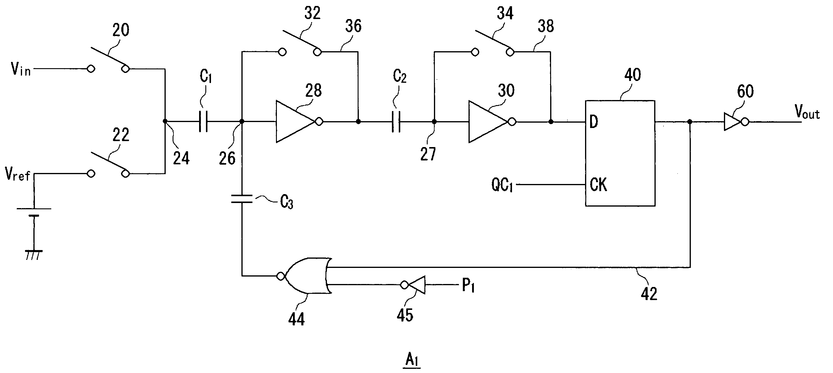
[0021] Conventional hysteresis circuits were achieved by switching the reference voltages to be input to their comparators. That is, it was necessary to provide at least two possible reference voltage signals, and a plurality of switches for switching the same. Those switches were analog switches, and thus had to be reduced in impedance as much as possible. For example, for AD conversion on a voltage value of 1 Vpp in 10 bits of resolution, 1 LSB was 0.98 mV. For AD conversion in 12 bits of resolution, 1 LSB=0.24 mV. Consequently, the greater the number of bits was, the smaller the bit-by-bit steps became in width. This facilitated noise-induced errors accordingly, with a drop in the conversion accuracy of the lower bits.

[0022] In the present embodiment, a hysteresis circuit is achieved by the configuration of applying pulses to an input stage of a chopper type comparator. As a result, small hysteresis can be realized by the simple configuration without providing a plurality of swi...

second embodiment

[0035] Comparators according to the present embodiment make basically the same operations as those of the comparators according to the first embodiment. Note that the comparators of the present embodiment, as shown in FIG. 6, are configured to include differential amplifiers. In other respects than the comparators, the present embodiment has the same circuit configuration as in the first embodiment. Description thereof will thus be omitted.

[0036]FIG. 6 shows the configuration of a comparator according to the second embodiment. In the first comparator A1, a first differential amplifier 50 and a second differential amplifier 52 are arranged in series. The first differential amplifier 50 corresponds to the first inverting circuit 28 in FIG. 3, and has differential input terminals and inverted differential output terminals. Similarly, the second differential amplifier 52 corresponds to the second inverting circuit 30 in FIG. 3, and has differential input terminals and inverted differen...

third embodiment

[0041] An AD conversion circuit according to the present embodiment is a pipelined AD conversion circuit.

[0042]FIG. 7 shows the configuration of the AD conversion circuit according to the third embodiment. The AD conversion circuit 200 is composed of s stages, which process AD conversion in several bits each. Here, the AD conversion circuit 200 includes a first stage 202, a second stage 204, a third stage 206, . . . , an sth stage 208. The first stage 202 converts input voltages Vin+ and Vin− into several bits of digital value, and transmits it to a signal generating circuit 210. The first stage 202 also subtracts the converted values from the original input values, amplifies the resultants, and transmits them to the second stage 204. Similarly, the second stage 204 converts the input values into several bits of digital value, and transmits it to the signal generating circuit 210. The second stage 204 subtracts the converted values from the original input values, amplifies the resu...


PUM


Abstract

A comparator is provided, which compares an input voltage and a reference voltage by using a plurality of inverting circuits connected in series. The comparator includes a first inverting circuit, a second inverting circuit, a feedback path, and a capacitor arranged on the feedback path. The first inverting circuit inverts a difference between the input voltage and the reference voltage for output. The second inverting circuit further inverts the output of the first inverting circuit for output. The feedback path feeds back the output of the second inverting circuit to the input side of the first inverting circuit. The capacitor causes hysteresis such that an increasing threshold and a decreasing threshold of the second inverting circuit corresponding to an increase and a decrease of the input voltage have a difference therebetween.

Description

BACKGROUND OF THE INVENTION [0001] 1. Field of the Invention [0002] The present invention relates to a comparator, an AD conversion circuit, a semiconductor device, and an image capturing apparatus. In particular, the invention relates to the technology of a hysteresis circuit to be formed in a comparator and an AD conversion circuit. [0003] 2. Description of the Related Art [0004] Conventionally, some comparators for use in multi-bit AD conversion circuits have incorporated a hysteresis circuit for reducing noise effect for the sake of improved operation stability (for example, see Japanese Patent Laid-Open Publication No. Hei 5-167400). The reason is that in multi-bit AD conversion circuits beyond 10 bits in particular, the increasing number of bits makes bit-by-bit voltage steps smaller and thus increases the possibility of noise-induced malfunctions. The conventional hysteresis circuit switches its reference voltage to a voltage value higher than a threshold when its input volta...

Claims


Application Information

Patent Timeline
Patent Type & Authority Applications(United States)
IPC IPC(8): H03K5/08H04N5/14H03K5/153H03K5/24H03M1/08H03M1/36H03M1/44H04N5/232
CPCH03K5/2481H03M1/365H03M1/0845H03K5/249H03K3/023H03F3/45H03M1/12H04N23/40
Inventor YUKI, HIROFUMIKAWAMURA, YASUNORI
Owner ROHM CO LTD
Why Eureka
Try Eureka