CMOS-process compatible high-DC surface coating for capacitive detection and stimulation of biological tissues

a capacitive detection and stimulation technology, applied in the field of biochips, to achieve the effect of convenient rinsing and straight cleaning

Active Publication Date: 2005-08-25
INFINEON TECH AG
View PDF1 Cites 9 Cited by
  • Summary
  • Abstract
  • Description
  • Claims
  • Application Information

AI Technical Summary

Benefits of technology

[0031] It has been shown that such smooth dielectric layers having TiO2 additionally afford the advantage of a straightforward cleaning capability. Preferably, surfaces for the growth of cell cultures should not only be smooth but also be completely accessible to cleaning solutions and readily rinsable. The dielectric layer of a biochip according to the invention is resistant in a wide pH range, so that it possible to use customary cleaning solutions for biological materials which in some instances have extreme pH values.
[0032

Problems solved by technology

It has been shown, however, that, in particular with regard to the coupling efficiency or the achievable signal transfer between stimulation and/or sensor de

Method used


Image

  • CMOS-process compatible high-DC surface coating for capacitive detection and stimulation of biological tissues
  • CMOS-process compatible high-DC surface coating for capacitive detection and stimulation of biological tissues
  • CMOS-process compatible high-DC surface coating for capacitive detection and stimulation of biological tissues

Examples


Embodiment Construction

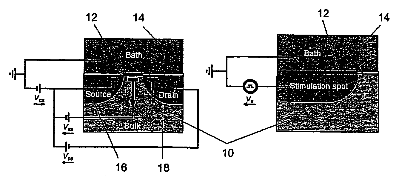
[0062]FIG. 1(a) illustrates an embodiment of a biochip according to the invention in a field-effect transistor circuitry, which is used as potential sensor. The biochip has a patterned structure 10, which is a semiconductor structure. The substrate of the semiconductor structure 10 is electrically contact-connected by means of an ohmic contact and electrically connected to a voltage source VBS. Arranged in the semiconductor structure 10 is a source contact 16 and also a drain contact 18 of a field-effect transistor, which are in each case electrically contact-connected. Arranged in the gate region of the field-effect transistor between the source contact 16 and the drain contact 18 is a dielectric layer having TiO2, which separates the semiconductor structure 10 from the electrolyte or the bath 14. The dielectric layer 12 thus constitutes the gate oxide of the field-effect transistor.

[0063] Consequently, the embodiment illustrated in FIG. 1 is a “laboratory prototype biochip” havin...


PUM


Abstract

Biochip for capacitive stimulation and/or detection of biological tissues. The biochip has a carrier structure, at least one stimulation and/or sensor device, which is arranged in or at the carrier structure, and at least one dielectric layer, one layer area of which is arranged at the stimulation and/or sensor device and the opposite layer area of which forms a stimulation and/or sensor area for capacitive simulation and/or detection of biological tissues, wherein the dielectric layer comprises TiO2.

Description

CROSS-REFERENCE TO RELATED APPLICATION [0001] This application is a continuation of International Patent Application Ser. No. PCT / EP03 / 01871, filed Feb. 24, 2003, which published in German on Sep. 12, 2003 as WO 03 / 074683, and is incorporated herein by reference in its entirety.FIELD OF THE INVENTION [0002] The invention relates to a biochip for capacitive stimulation and / or detection of biological tissues and to a method for producing a corresponding biochip. BACKGROUND OF THE INVENTION [0003] On the laboratory scale, it has already been a good ten years since direct communication between nerve cells and electrically active solid-state structures, such as e.g. semiconductors, left the realm of fiction. Successful laboratory experiments have been reported for example by P. Fromherz et al. in Science 252, 1290 (1991); P. Fromherz et al. in Physical Review Letters 75, 1670 (1995) and also P. Stett et al. in Physical Review E Vol. 55, No. 2, 1779 (1997). A summary overview of the early...

Claims


Application Information

Patent Timeline
IPC IPC(8): B01L3/00C12N5/06C12N5/0793G01N27/414G01N33/00G01N33/487G01N33/543
CPCG01N33/4833C12N5/0619
Inventor GABL, REINHARDBIRKENMAIER, TAMARAEVERSMANN, BJORN-OLIVERFROMHERZ, PETERJENKNER, MARTINSCHREITER, MATTHIASTHEWES, ROLANDWERSING, WOLFRAM
Owner INFINEON TECH AG
Why Eureka
Try Eureka