Self-assembly organic dielectric layers based on phosphonic acid derivatives

a technology of organic dielectric layers and phosphonic acid derivatives, applied in the field of transistors, can solve problems such as the cost of construction and connection technology

Inactive Publication Date: 2005-09-01
QIMONDA
View PDF8 Cites 31 Cited by
  • Summary
  • Abstract
  • Description
  • Claims
  • Application Information

AI Technical Summary

Benefits of technology

[0007] An object of the present invention is to provide new classes of compounds that can serve as a monomolecular dielectrics for use in field effect transistors based on organic semiconductors.

Problems solved by technology

These transponders are usually produced using integrated circuits based on monocrystalline silicon, which leads to considerable costs in the construction and connection technology.

Method used


Image

  • Self-assembly organic dielectric layers based on phosphonic acid derivatives
  • Self-assembly organic dielectric layers based on phosphonic acid derivatives
  • Self-assembly organic dielectric layers based on phosphonic acid derivatives

Examples


Embodiment Construction

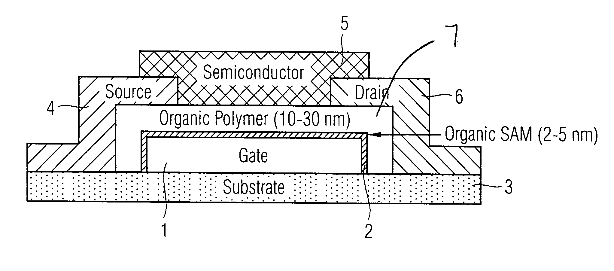
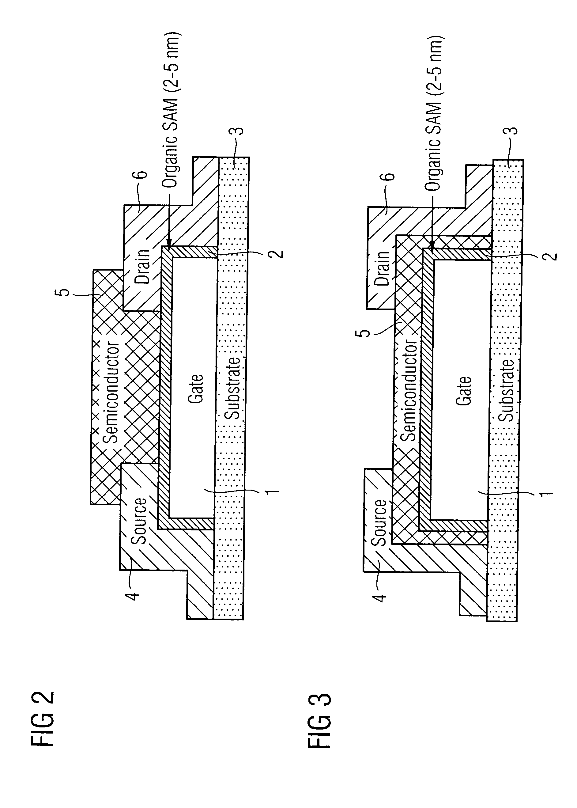
[0031] In accordance with the present invention, a field effect transistor (FET) is constructed including a substrate with a source electrode, a drain electrode, a gate electrode, and a semiconductor material. The FET further includes a dielectric layer (gate dielectric) formed from a self-assembled monolayer of an organic compound arranged on the gate electrode, where the organic compound includes a phosphoric acid group.

[0032] The dielectric layers formed according to the invention are so stable that it is possible to carry out photolithography processes on their surfaces such as, for example, deposition and patterning of further metal layers, deposition of an organic or inorganic semiconductor, etc. Electronic components, such as organic field effect transistors, for example, can thus be fabricated and be extended to form integrated circuits.

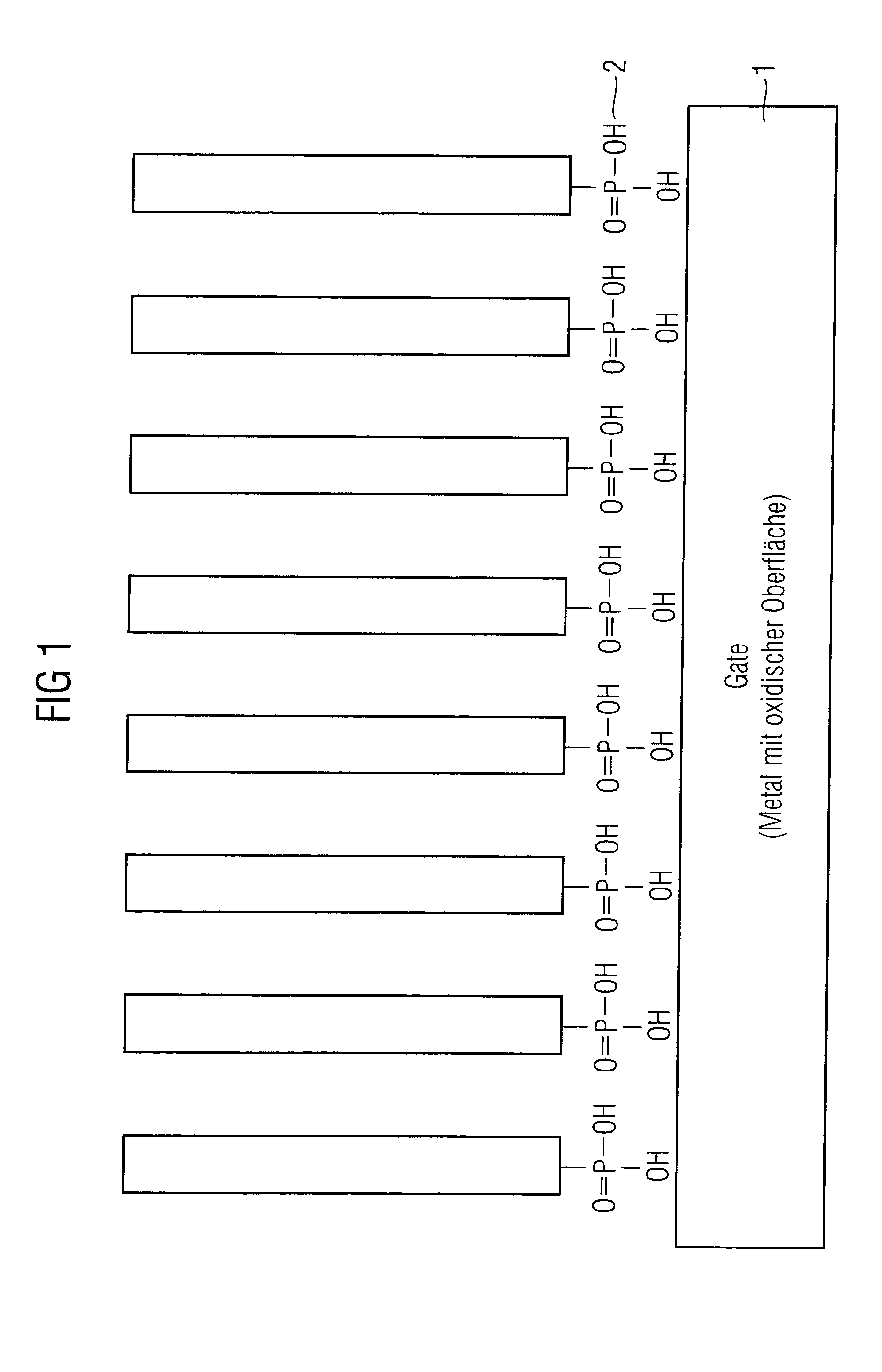
[0033] In an exemplary embodiment, the organic compound of the FET has the following formula I: [0034] where: [0035] M comprises at least...


PUM


Abstract

A field effect transistor includes a gate dielectric with a self-assembled monolayer of an organic compound, where the organic compound includes a phosphonic acid group. The phosphonic acid group additionally has an organic radical selected from the group consisting of (a) an alkyl chain including 1 to 20 carbon atoms, (b) oligo(thio)ether chains and/or c) aromatic or heteroaromatic compounds. In addition, a method for fabricating a field effect transistor includes forming a self-assembled monolayer of an organic compound as a gate dielectric, where the organic compound includes a phosphonic acid group.

Description

CROSS REFERENCE TO RELATED APPLICATIONS [0001] This application claims priority under 35 USC §119 to German Application No. DE 10 2004 009 600.7, filed on Feb. 27, 2004, and titled “Self-Assembly Organic Dielectric Layers Based on Phosphonic Acid Derivatives,” the entire contents of which are hereby incorporated by reference. FIELD OF THE INVENTION [0002] The invention relates to transistors, in particular field effect transistors, including organic dielectric layers. BACKGROUND [0003] High-quality, extremely thin dielectric layers are of considerable interest for a multiplicity of applications. In particular, the realization of inexpensive electronics on large-area flexible substrates that operate with low supply voltages requires the availability of such layers for constructing transistors, capacitors, etc. By way of example, organic field effect transistors are suitable as pixel control elements in active matrix screens. Such screens are usually produced with field effect transis...

Claims


Application Information

Patent Timeline
Patent Type & Authority Applications(United States)
IPC IPC(8): H01L21/28H01L29/08H01L29/49H01L29/51H01L51/00H01L51/30
CPCB82Y10/00B82Y30/00H01L51/0516H01L29/4908H01L29/51H01L21/28194H10K10/468
Inventor ZSCHIESCHANG, UTEKLAUK, HAGENHALIK, MARCUSSCHMID, GUENTER
Owner QIMONDA
Why Eureka
Try Eureka