Electronic component, method of manufacturing the electronic component, and electronic apparatus

a manufacturing method and electronic component technology, applied in the direction of electrical apparatus casings/cabinets/drawers, coupling device connections, semiconductor/solid-state device details, etc., can solve the problems of high sensitivity, high price of components, and high cost of mounting devices, so as to reduce the price of electronic devices and simplify the mounting process , the effect of easy mounting

Active Publication Date: 2005-09-01
ADVANCED INTERCONNECT SYST LTD
View PDF6 Cites 2 Cited by
  • Summary
  • Abstract
  • Description
  • Claims
  • Application Information

AI Technical Summary

Benefits of technology

[0032] The electronic component manufactured by this method, which does not require the discrimination between the front face and the bottom face of the substrate, can adopt a mounting method by using vibration positioning in which the electronic components are guided to predetermined positions on a mount board while the electronic components are vibrated or a mounting method by using external-shape positioning in which the electronic components are fit in predetermined positions based on their external shapes. Hence, there is no need to use an expensive mounter, thus largely simplifying the mounting process. As a result, it is possible to reduce the price of the electronic apparatus, such as an IC card, which includes a small number of electronic components to be mounted but which is manufactured in large quantities. Furthermore, the price of a display device that uses a large display, such as an OLED, a PDP, or an LCD, and that has a large number of data drivers mounted therein can also be reduced.
[0033] The present invention provides, in its third aspect, an electronic apparatus in which any of the electronic components described above is mounted. Since the electronic component can be easily mounted in the electronic apparatus in various manners, it is possible to reduce the size and cost of the electronic apparatus. Furthermore, the electronic apparatus in which the electronic component having the outer electrodes and the interconnection lines formed on their stress relief layers is mounted can improve its reliability and / or lengthen its life as the reliability of the electronic component is improved.

Problems solved by technology

Mounters are expensive because they have components requiring high precision and high sensitivity.
Hence, an electronic apparatus manufactured by mounting the electronic components by using such an expensive mounter is also expensive.
As a result, the price of the electronic apparatus, for example, an integrated circuit (IC) card, which includes a small number of electronic components to be mounted but which is manufactured in large quantities, is increased.
When it is necessary to use the expensive mounter described above in this type of display device, despite the fact that a higher mount precision of the data drivers is not required, the price of the display device becomes expensive.
Furthermore, there are problems in reduction of the reliability and / or shortening of the life due to thermal stress in known semiconductor devices.

Method used


Image

  • Electronic component, method of manufacturing the electronic component, and electronic apparatus
  • Electronic component, method of manufacturing the electronic component, and electronic apparatus
  • Electronic component, method of manufacturing the electronic component, and electronic apparatus

Examples


first embodiment

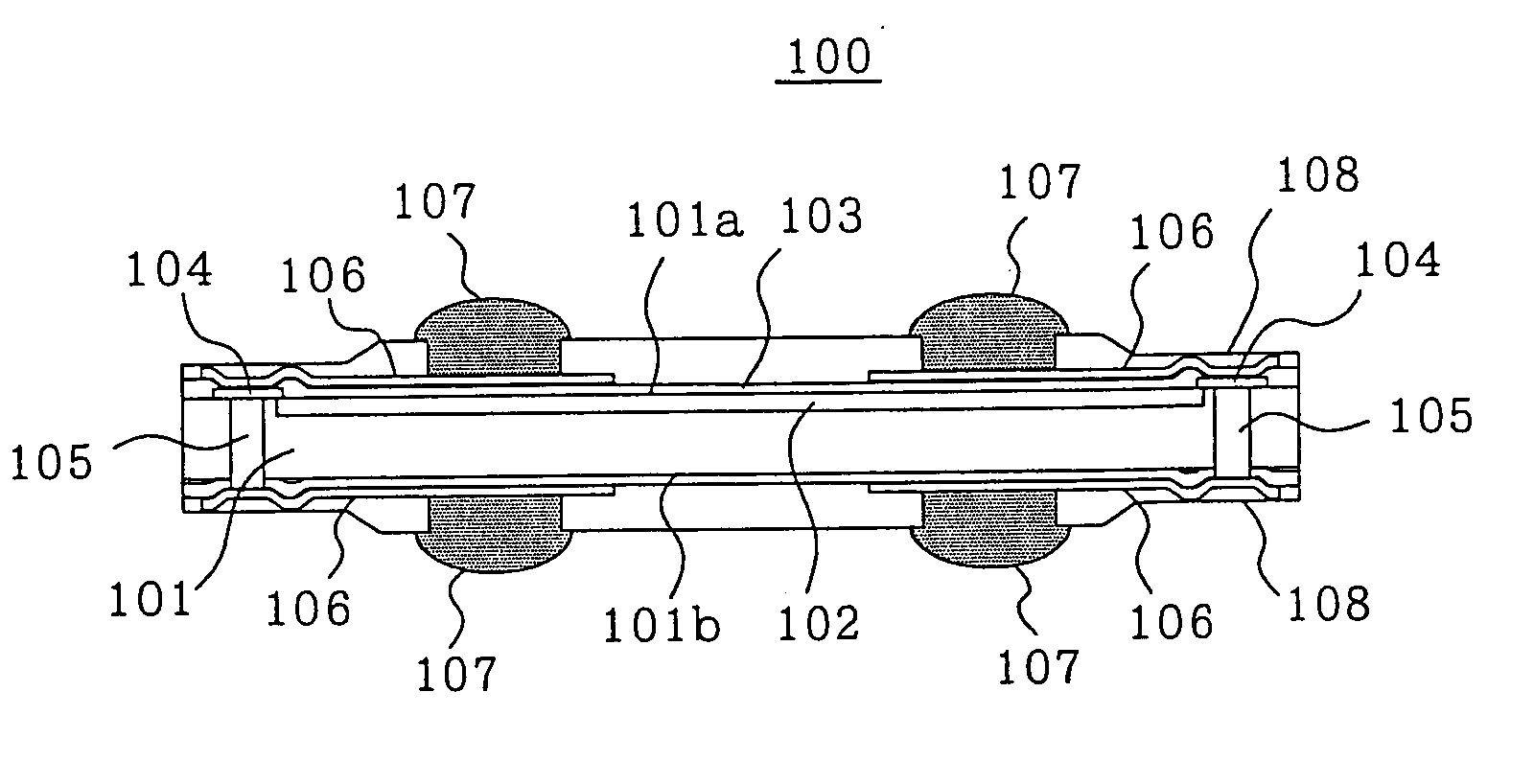
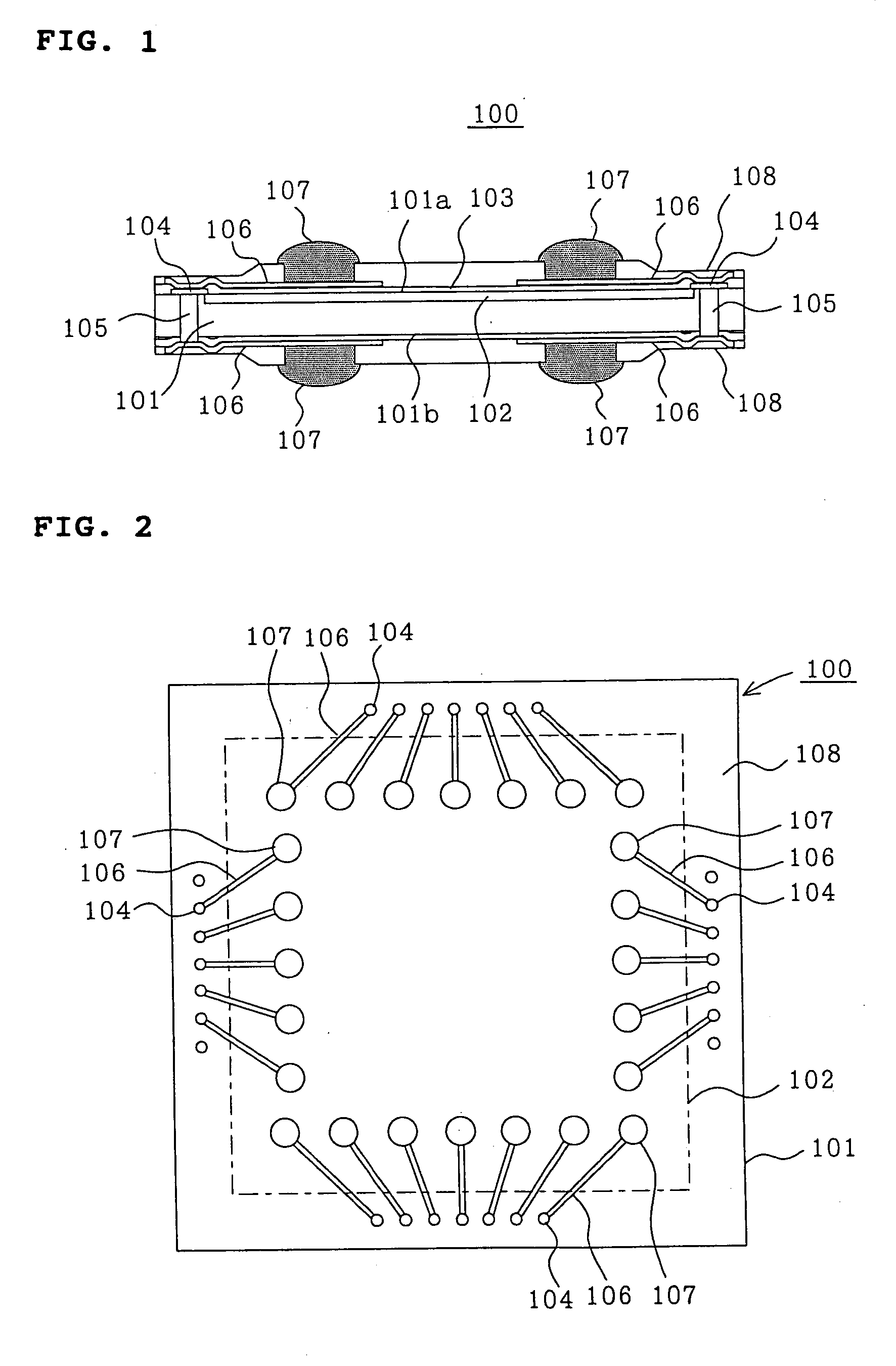
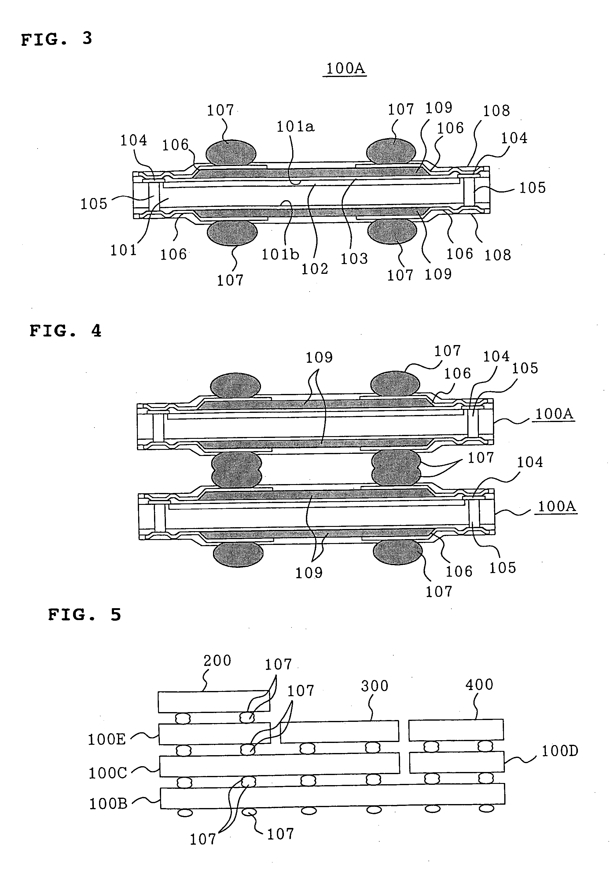
[0047]FIG. 1 is a sectional view showing the structure of a semiconductor device 100, which is an electronic component according to a first embodiment of the present invention. FIG. 2 is a plan view showing the front face of the electronic component shown in FIG. 1. The semiconductor device 100 has a silicon substrate 101. A functional part 102 is formed beneath a front face 101a of the silicon substrate 101. A passivation layer 103, made of silicon nitride (SiN), silicon oxide (SiO), or the like, is preferably formed on the functional part 102. The functional part 102 has a single active element or at least one active element and at least one passive element. In order to carry out a predetermined function, the functional part 102 performs a variety of signal processing, including arithmetic processing, image processing, speech synthesis, sound analysis, noise reduction, frequency analysis, encryption, decryption, and authentication, for input signals supplied from input terminals t...

second embodiment

[0057]FIG. 6 is a schematic top view of a semiconductor device 1, which is an electronic component according to a second embodiment of the present invention. FIG. 7 is a schematic bottom view of the semiconductor device 1 in FIG. 6. FIG. 8 is a cross-sectional view of the semiconductor device 1 in FIG. 6 taken along line X-X′.

[0058] The semiconductor device 1 has a rectangular silicon substrate 2 and a functional part 3. The functional part 3 is formed beneath a substantially central part of a front face 2a and in the vicinity of the front face 2a of the silicon substrate 2. Outer electrodes 61 to 620 are formed near the margin of the front face 2a of the silicon substrate 2. Outer electrodes 71 to 720 are formed near the margin of a bottom face 2b of the silicon substrate 2. The outer electrodes 61 to 620 are hereinafter collectively referred to as outer electrodes 6. The same applies to the outer electrodes 71 to 720 and other components whose reference numerals have subscripts. ...

third embodiment

[0079]FIG. 11 is a schematic cross-sectional view showing the structure of a semiconductor device 21, which is an electronic component according to a third embodiment of the present invention. The same reference numerals are used in FIG. 11 to identify the same components shown in FIGS. 6 to 8. A detailed description of such components is omitted here. In the semiconductor device 21 shown in FIG. 11, a stress relief layer 221 having a substantially trapezoidal cross section is formed on the substantially central part of the front face 2a of the silicon substrate 2. In addition, a stress relief layer 222 having the same shape as the stress relief layer 221 is formed on the substantially central part of the bottom face 2b of the silicon substrate 2. The stress relief layer 221 is plane symmetric with the stress relief layer 222 with respect a virtual plane including the midpoint between the front face 2a and the bottom face 2b of the silicon substrate 2. The stress relief layer 221 an...


PUM


Abstract

An electronic component includes a substrate; a functional part that is formed beneath at least one of a front face and a bottom face of the substrate and that performs a predetermined function; a plurality of terminals that is formed on the front face or the bottom face of the substrate and that is connected to the functional part; a plurality of outer electrodes formed on the front face and the bottom face of the substrate; and interconnection lines, formed on the front face and the bottom face of the substrate, for connecting the terminals on the front face or the bottom face of the substrate to the outer electrodes.

Description

CROSS-REFERENCE TO RELATED APPLICATIONS [0001] The entire disclosures of Japanese Patent Application Nos. 2004-33028-9 filed Nov. 15, 2004 and 2004-004692 filed Jan. 9, 2004 are hereby incorporated by reference. BACKGROUND OF THE INVENTION [0002] 1. Field of the Invention [0003] The present invention relates to an electronic component, such as a semiconductor device, which is a module having a single active device or at least one active element and at least one passive element, to a method of manufacturing the electronic component, and to an electronic apparatus in which the electronic component is mounted. [0004] 2. Description of the Related Art [0005] A known semiconductor device has a semiconductor element having through-holes formed at the positions of electrodes, insulating materials provided in areas including the inner sides of the through-holes, and conductive members provided around the central axes of the through-holes (for example, refer to Japanese Unexamined Patent App...

Claims


Application Information

Patent Timeline
Patent Type & Authority Applications(United States)
IPC IPC(8): H01G4/228H01L23/52H01L21/3205H01L21/60H01L21/77H01L21/822H01L23/12H01L23/31H01L23/48H01L23/485H01L25/065H01L25/07H01L25/10H01L25/18H01L27/04
CPCH01L23/3114H01L23/481H01L2224/13144H01L2224/13111H01L2224/131H01L2924/12041H01L2225/1058H01L2924/014H01L24/17H01L25/0652H01L25/0657H01L25/105H01L2224/13099H01L2225/06513H01L2225/06524H01L2225/06541H01L2924/01002H01L2924/01013H01L2924/01029H01L2924/01033H01L2924/01051H01L2924/01074H01L2924/01079H01L2924/01082H01L2924/12044H01L2924/14H01L24/13H01L2924/01005H01L2924/01006H01L2924/01047H01L2924/00014H01L2924/01028H01L2924/351H01L2224/05024H01L2224/02372H01L2224/05009H01L2224/05548H01L2224/05023H01L2224/05001H01L2224/06135H01L2224/02377H01L24/05H01L2924/00H01L2224/05599H01L2224/05099H02G3/06Y10S174/08
Inventor HASHIMOTO, NOBUAKI
Owner ADVANCED INTERCONNECT SYST LTD
Why Eureka
Try Eureka