Method for fabricating a field effect transistor

a field effect transistor and transistor technology, applied in the direction of electrical equipment, semiconductor devices, material nanotechnology, etc., can solve the problem of short circuits

Inactive Publication Date: 2005-09-01
POLARIS INNOVATIONS
View PDF2 Cites 6 Cited by
  • Summary
  • Abstract
  • Description
  • Claims
  • Application Information

AI Technical Summary

Benefits of technology

[0008] The present invention provides a method for fabricating a field effect transistor which has fewer process steps than conventional methods and additionally enables the fabrication of a field effect transistor which can be operated at a supply voltage of less than 5 volts, and in particular, less than three volts.

Problems solved by technology

Such a short circuit can occur if the molecular wetting of the gate electrode along the vertical etching edges is insufficient, after the etching of the gate layer.

Method used


Image

  • Method for fabricating a field effect transistor
  • Method for fabricating a field effect transistor
  • Method for fabricating a field effect transistor

Examples


Embodiment Construction

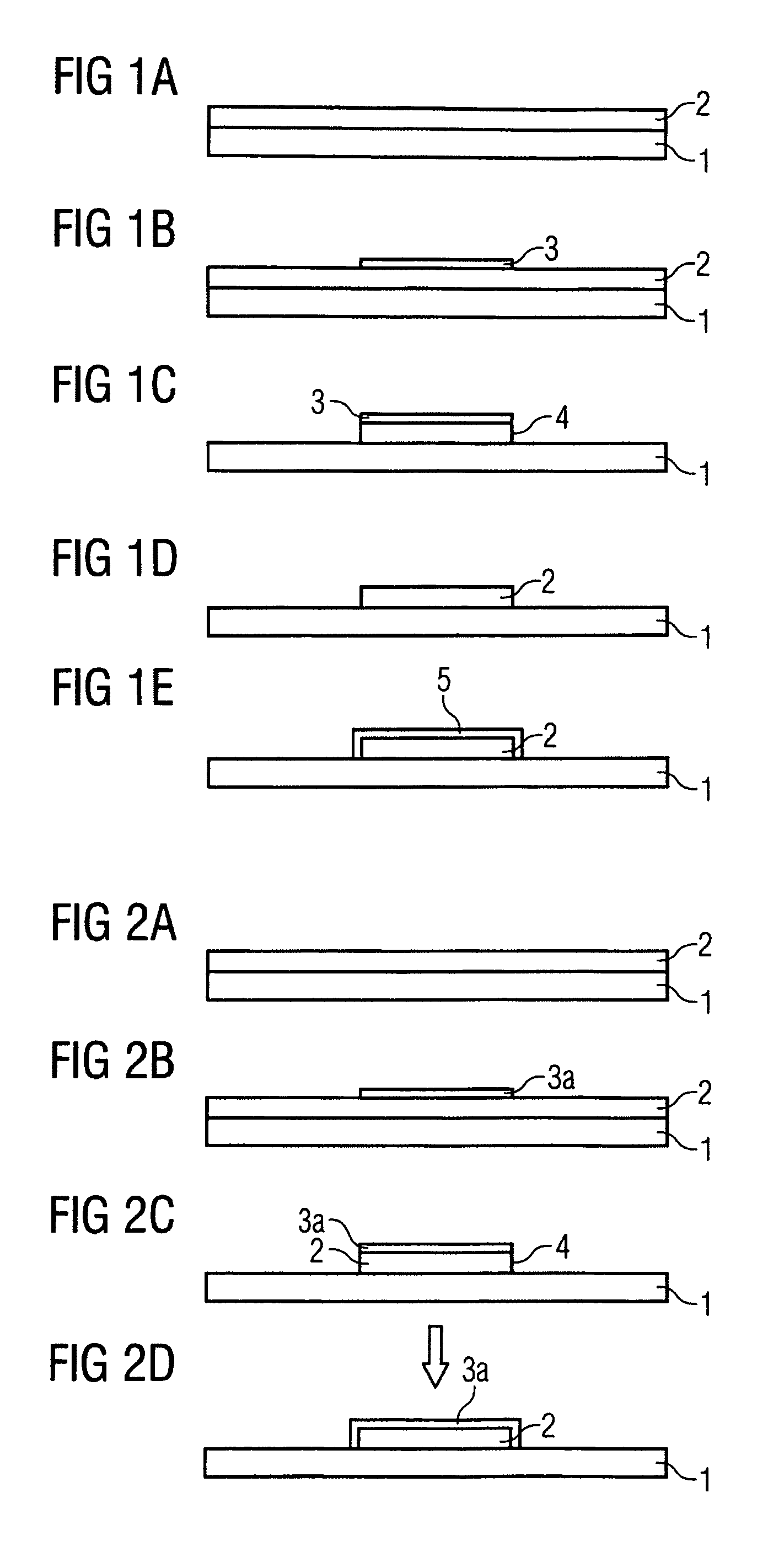
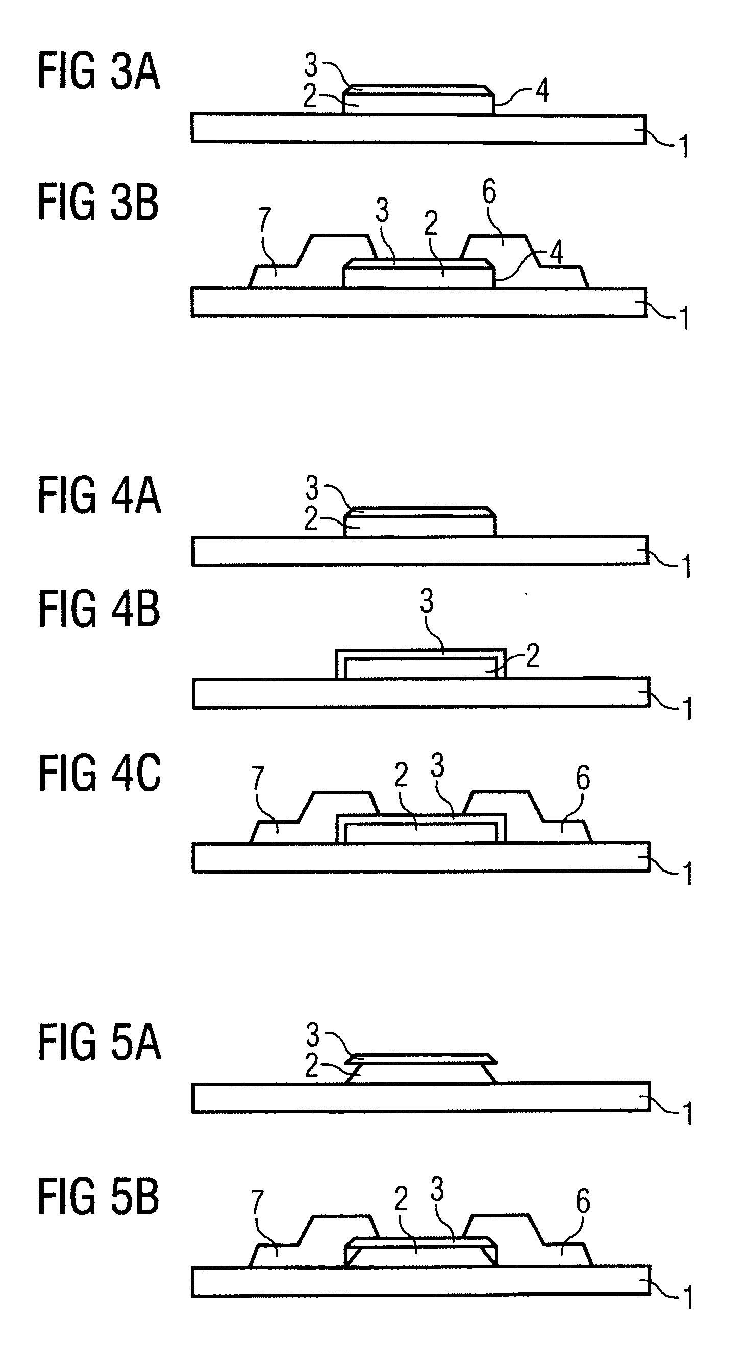
[0036]FIG. 1 illustrates the necessary steps in the fabrication of a conventional field effect transistor. In FIG. 1a, a layer 2 of a material used for the fabrication of the gate electrode is deposited on a substrate 1. As illustrated in FIG. 1b, an etching mask 3 is thereupon deposited onto the layer of gate electrode 2, preferably by means of a printing technique. FIG. 1c illustrates the result after the etching step and the patterning of the gate electrode. It can be seen from FIG. 1c that the etching edges 4 are uncovered.

[0037] In FIG. 1d, the etching mask 3 then has to be removed before a dielectric 5 is deposited above the gate electrode.

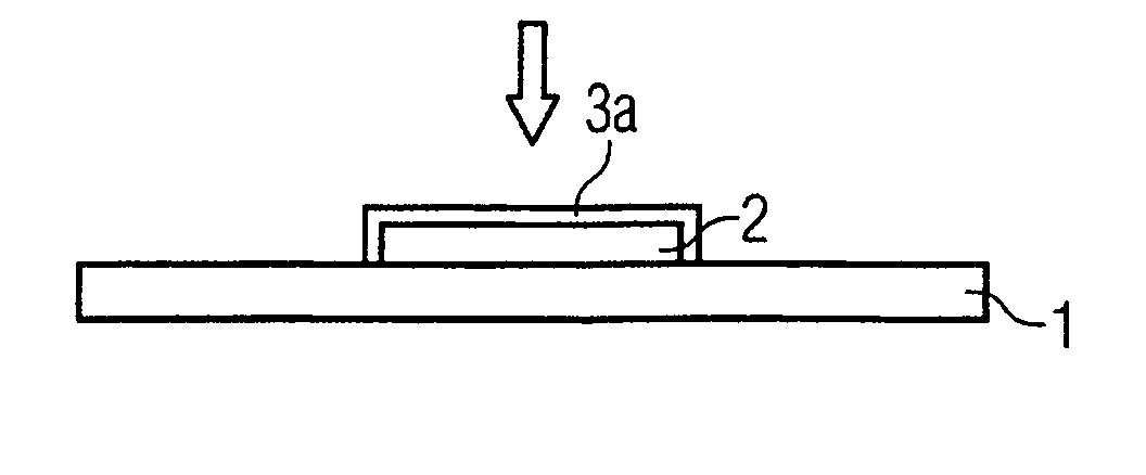
[0038] In accordance with the method according to the invention, it can be seen that the step of removing the etching mask 3 is completely omitted since the self-assembled molecular monolayer of the organic compound 3a serves both as the etching mask 3 and as the dielectric layer 5 for the subsequent process. The process sequences, compara...


PUM


Abstract

A method for fabricating a field effect transistor, in which, after the etching of the gate electrode, the removal of the etching mask is omitted since the etching mask serves as a gate dielectric. The etching mask or the dielectric has a self-assembled monolayer of an organic compound.

Description

CROSS REFERENCE TO RELATED APPLICATIONS [0001] This application claims priority under 35 USC § 119 to German Application No. DE 10 2004 009 601.5, filed on Feb. 27, 2004, and titled “Method for Fabricating a Field Effect Transistor,” the entire contents of which are hereby incorporated by reference. BACKGROUND [0002] Field effect transistors based on organic semiconductors are of interest for a multiplicity of electronic applications requiring extremely low production costs, flexible or unbreakable substrates, or the fabrication of transistors and integrated circuits over a large active area. For example, organic field effect transistors are suitable as pixel control elements in active matrix screens. Such screens are usually produced with field effect transistors based on amorphous or polycrystalline silicon layers. Typically, temperatures of more than 250° C. are necessary for fabricating high-quality transistors, which are based on amorphous or polycrystalline silicon layers requ...

Claims


Application Information

Patent Timeline
Patent Type & Authority Applications(United States)
IPC IPC(8): H01L21/336H01L21/8234H01L51/05H01L51/10H01L51/40
CPCB82Y10/00B82Y30/00H01L51/102H01L51/0541H01L51/0545H01L51/0512H10K10/462H10K10/464H10K10/82H10K10/466
Inventor ZSCHIESCHANG, UTEKLAUK, HAGENHALIK, MARCUSSCHMID, GUENTERBRAUN, STEFAN
Owner POLARIS INNOVATIONS
Why Eureka
Try Eureka