Method for production of a semiconductor structure

a semiconductor and structure technology, applied in the direction of photomechanical treatment, instruments, electrical equipment, etc., can solve the problems of lithographic patterning, cost and feature size, and each lithographic step or each lithographic level is expensive and complex,

Inactive Publication Date: 2005-09-08
POLARIS INNOVATIONS
View PDF13 Cites 13 Cited by
  • Summary
  • Abstract
  • Description
  • Claims
  • Application Information

AI Technical Summary

Benefits of technology

[0007] One advantage of the invention is that only a single lithography level for patterning the upper, third mask layer is required to transfer two different trench structures into a semiconductor substrate.
[0008] In one embodiment of the invention, the window is transferred in the upper, third mask layer into the mask layers beneath it and in widening this window at a defined location in a self-aligning manner using a maskless process step and also transferring the widened window into the mask layers below, and in patterning the substrate using the window and the widened window in succession.
[0009] According to a preferred embodiment, the patterning of the lower, first mask layer using the first window in the middle, second mask layer in order to transfer the first window into the lower, first mask layer and the increasing of the size of the first window in the upper, third mask layer are carried out simultaneously in a single etching step which is selective with respect to the semiconductor substrate and with respect to the middle, second mask layer.
[0010] According to a further preferred embodiment, the patterning of the semiconductor substrate using the patterned lower, third mask layer and the repatterning of the middle, second mask layer using the second window in the upper, third mask layer in order to transfer the second window into the middle, second mask layer are carried out simultaneously in a single etching step which is selective with respect to the lower, first mask layer and with respect to the middle, second mask layer.
[0011] According to a further preferred embodiment, during the patterning of the semiconductor substrate a first trench is created, and during the repatterning of the semiconductor substrate a second, wider and shallower trench is created.
[0012] According to a further preferred embodiment, the semiconductor substrate consists of silicon oxide, the lower, first mask layer consists of carbon, the middle, second mask layer consists of silicon oxynitride, and the upper, third mask layer consists of photoresist.

Problems solved by technology

Each lithography step or each lithography level is expensive and complex.
As well as costs and feature size, another limiting factor in lithographic patterning is the accuracy of the vertical alignment of two or more lithography levels located above one another.

Method used


Image

  • Method for production of a semiconductor structure
  • Method for production of a semiconductor structure
  • Method for production of a semiconductor structure

Examples


first embodiment

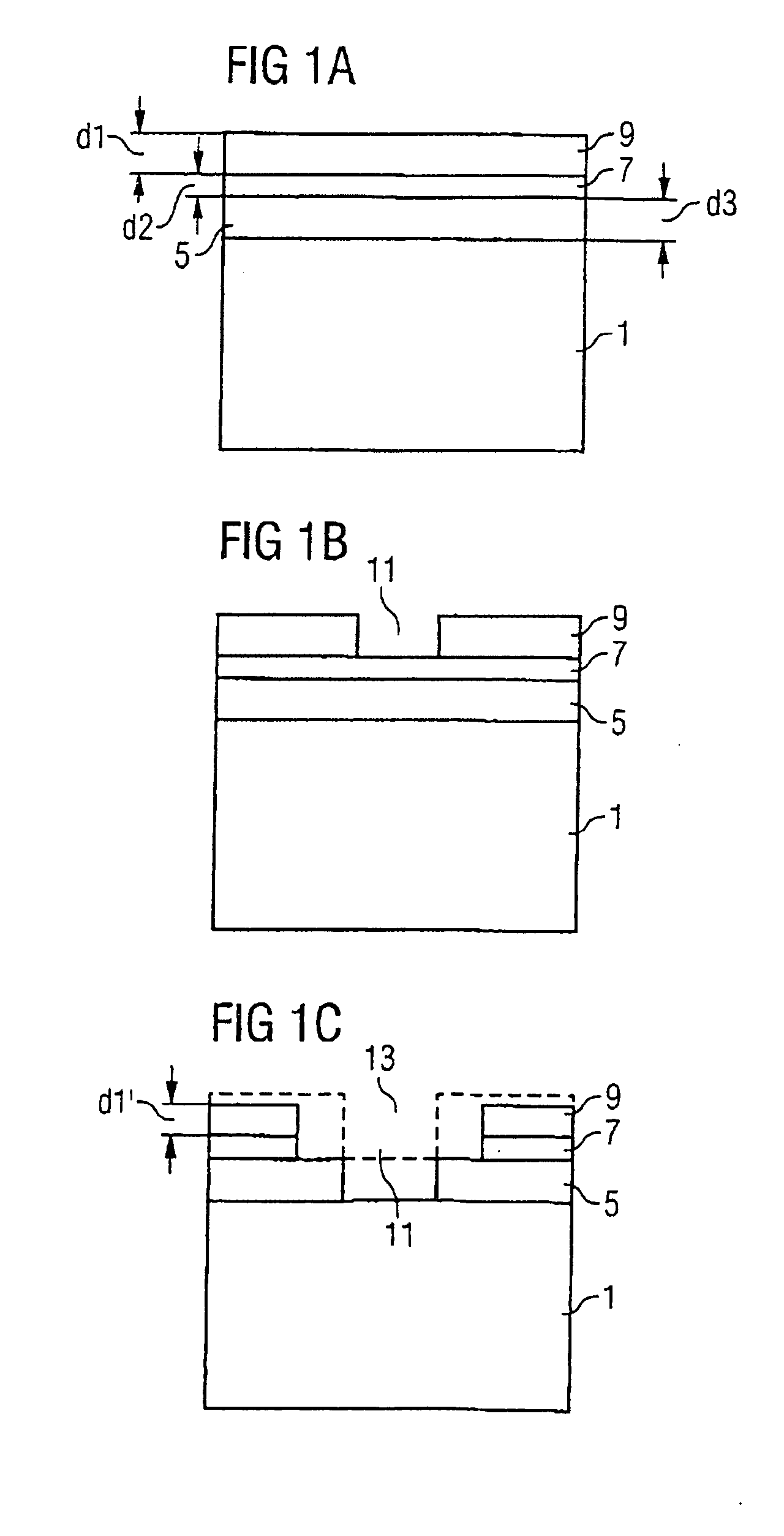
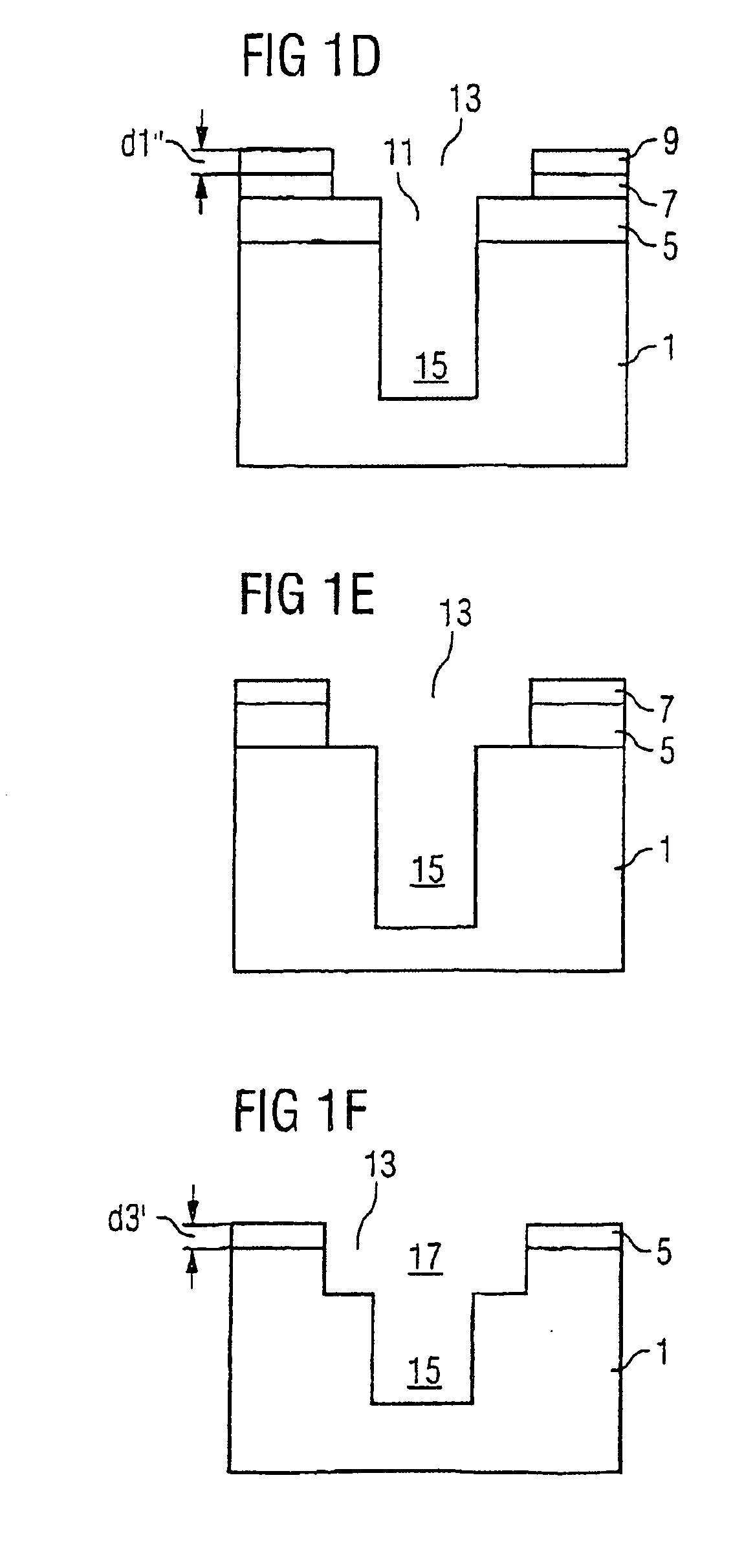
[0026]FIGS. 1a-f show successive method stages involved in a method for production of a semiconductor structure as the present invention.

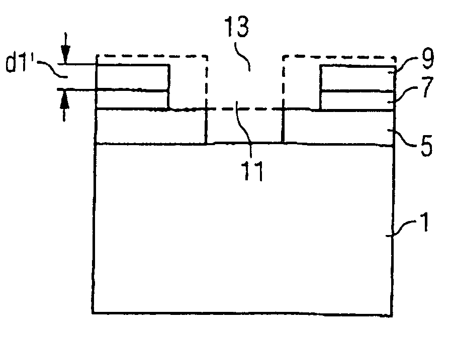
[0027] In FIG. 1a, reference numeral 1 denotes a semiconductor substrate of silicon oxide (SiO2). For reasons of simplicity, this semiconductor substrate 1 is shown without a silicon wafer beneath it or other layers beneath it, to which the silicon oxide semiconductor structure 1 has been applied by an oxidation process, a deposition process, an epitaxy process, a direct-bonding process or the like.

[0028] In a first method step, a lower, first mask layer 5 of carbon with a thickness d3, a middle, second mask layer 7 of silicon oxynitride with a thickness d2 and an upper, third mask layer 9 of photoresist with a thickness d1 are provided on the semiconductor substrate 1. It is customary for the mask layers 5 and 7 to be deposited and for the mask layer 9 to be spun on.

[0029] Then, referring to FIG. 1b, a first window 11 is formed in the upper, thi...

second embodiment

[0041]FIGS. 2a-f show successive method stages involved in a method for production of a semiconductor structure as the present invention.

[0042] The second embodiment shown in FIGS. 2a to 2h illustrates that highly advantageous interlinked structures can be formed in the plane of the mask layers by the invention. FIGS. 2a to 2h illustrate this by means of a plan view of the top side of the semiconductor substrate 1, on which the three mask layers 5, 7, 9 are located. FIGS. 2a to 2h correspond to their associated pair in FIGS. 1a to 1h.

[0043] As shown in FIG. 2a, in the initial stage the entire surface is covered with the top, third mask layer 9 of photoresist.

[0044] Then, referring now to FIG. 2b, a plurality of first windows 11a to 11h are formed in the upper, third mask layer 9 of photoresist using the exposure mask (not shown) in the customary lithography step. To establish the paired relationship between FIGS. 1a to 1h and FIGS. 2a to 2h, it can be imagined that FIGS. 1a to 1h ...


PUM


Abstract

A method for producing a semiconductor structure including preparing a semiconductor substrate, and generating a lower first, a middle second and an upper third masking layer on a surface of the semiconductor substrate. The method further includes forming at least one first window in the upper third masking layer, structuring the middle second masking layer using the first window for transferring the first window, structuring the lower first masking layer using the first window for transferring the first window, and enlarging the first window to form a second window. The method for further includes restructuring the middle second masking layer using the second window for transferring the second window, structuring the semiconductor substrate, using the structured lower third masking layer, restructuring the lower first masking layer using the second window, and restructuring the semiconductor substrate using the restructured lower third masking layer.

Description

CLAIM FOR PRIORITY [0001] This application is a continuation of PCT / EP2003 / 009551, published in the German language on Mar. 25, 2004, which claims the benefit of priority to German Application No. 102 40 099.7, filed on Aug. 30, 2002.TECHNICAL FIELD OF THE INVENTION [0002] The present invention relates to a method for production of a semiconductor structure. BACKGROUND OF THE INVENTION [0003] Although in principle applicable to any integrated circuits, the present invention and the problems on which it is based are explained with reference to semiconductor structures in silicon technology. [0004] The patterning of semiconductor structures in silicon technology is effected by alternate production of masks, e.g. by exposing and developing photoresist layers, and dry-chemical or wet-chemical isotropic or anisotropic etching. Each lithography step or each lithography level is expensive and complex. Therefore, the aim of semiconductor fabrication is to minimize the number of lithography ...

Claims


Application Information

Patent Timeline
Patent Type & Authority Applications(United States)
IPC IPC(8): H01L21/027H01L21/033H01L21/308H01L21/311H01L21/4763H01L21/768H01L21/8234H01L21/8244
CPCH01L21/76811H01L21/0276H01L21/31144H01L21/3081H01L21/0332
Inventor GENZ, OLIVERKIRCHHOFF, MARKUSMACHILL, STEFANREB, ALEXANDERSCHMIDT, BARBARASTAVREV, MOMTCHILSTEGEMAN, MAIKWEGE, STEPHAN
Owner POLARIS INNOVATIONS
Why Eureka
Try Eureka