

Semiconductor device
a technology of semiconductor devices and semiconductors, applied in semiconductor devices, digital storage, instruments, etc., can solve the problem of ten-times the cost of a bit, and achieve the effect of reducing the cost per bit and effectively simplifying the production process
- Summary
- Abstract
- Description
- Claims
- Application Information
AI Technical Summary
Benefits of technology
Problems solved by technology
Method used
Image

Examples
embodiment 2
[Embodiment 2]
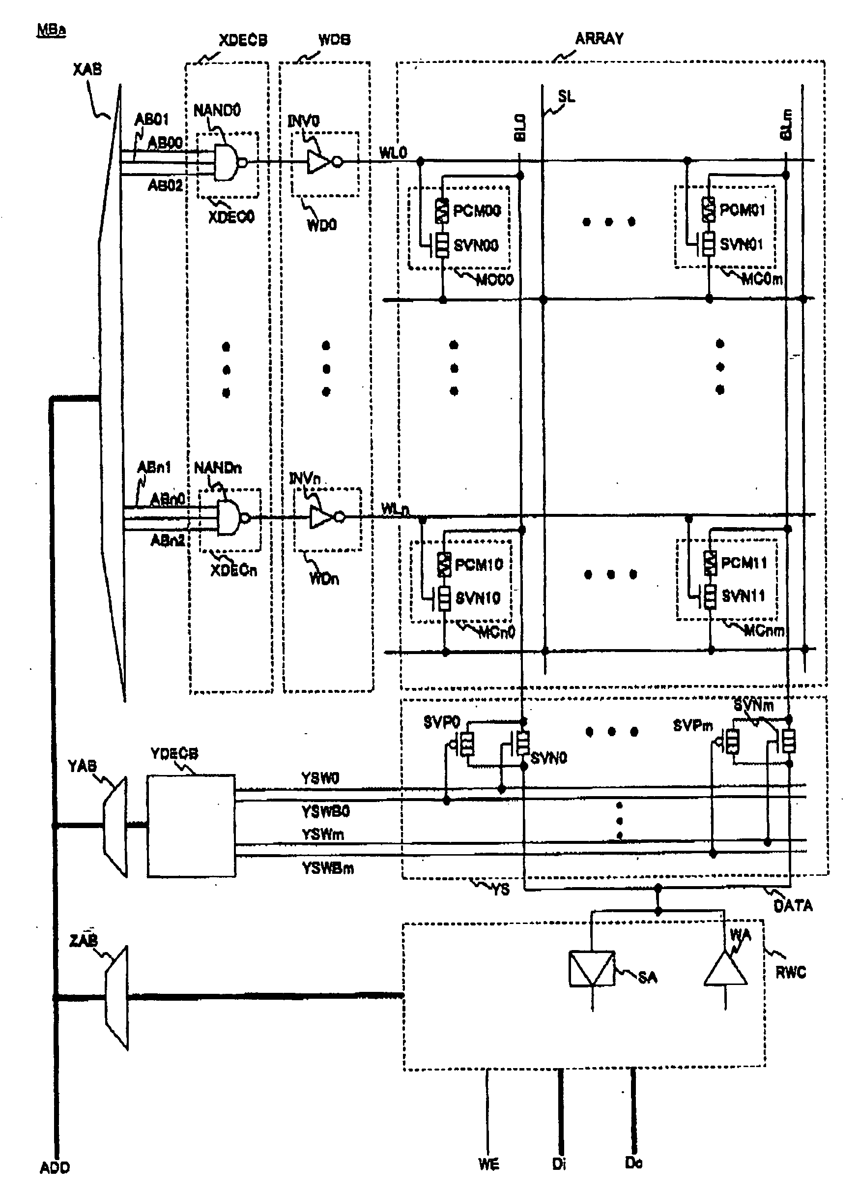
[0053] In Embodiment 1, a memory block layer comprised of only vertical MOS transistors are laminated, however, a part of the circuit of the memory block layer may be disposed on silicon substrate Si. In this embodiment, a case in which an address buffer block AB, Y-address decoder block YDECB, and read / write circuit RWC are disposed on a silicon substrate Si, is explained. Herein, a Z-circuit is configured so as to be integrated with a Y-circuit.
[0054] A detailed circuit diagram of a memory block layer MBb is shown in FIG. 9. The memory block layer MBb is comprised of only a memory array ARRAY, an X-address decoder block XDECB, a word driver block WDB, and a column selection circuit YS, with the indirect peripheral circuit removed from the memory block layer described in Embodiment 1. All circuits are formed by employing vertical transistors.
[0055] Four layers (MB0, MB1, MB2, and MB3) of the memory block layer MBb are laminated on a silicon substrate Si, and periphe...
embodiment 3
[Embodiment 3]
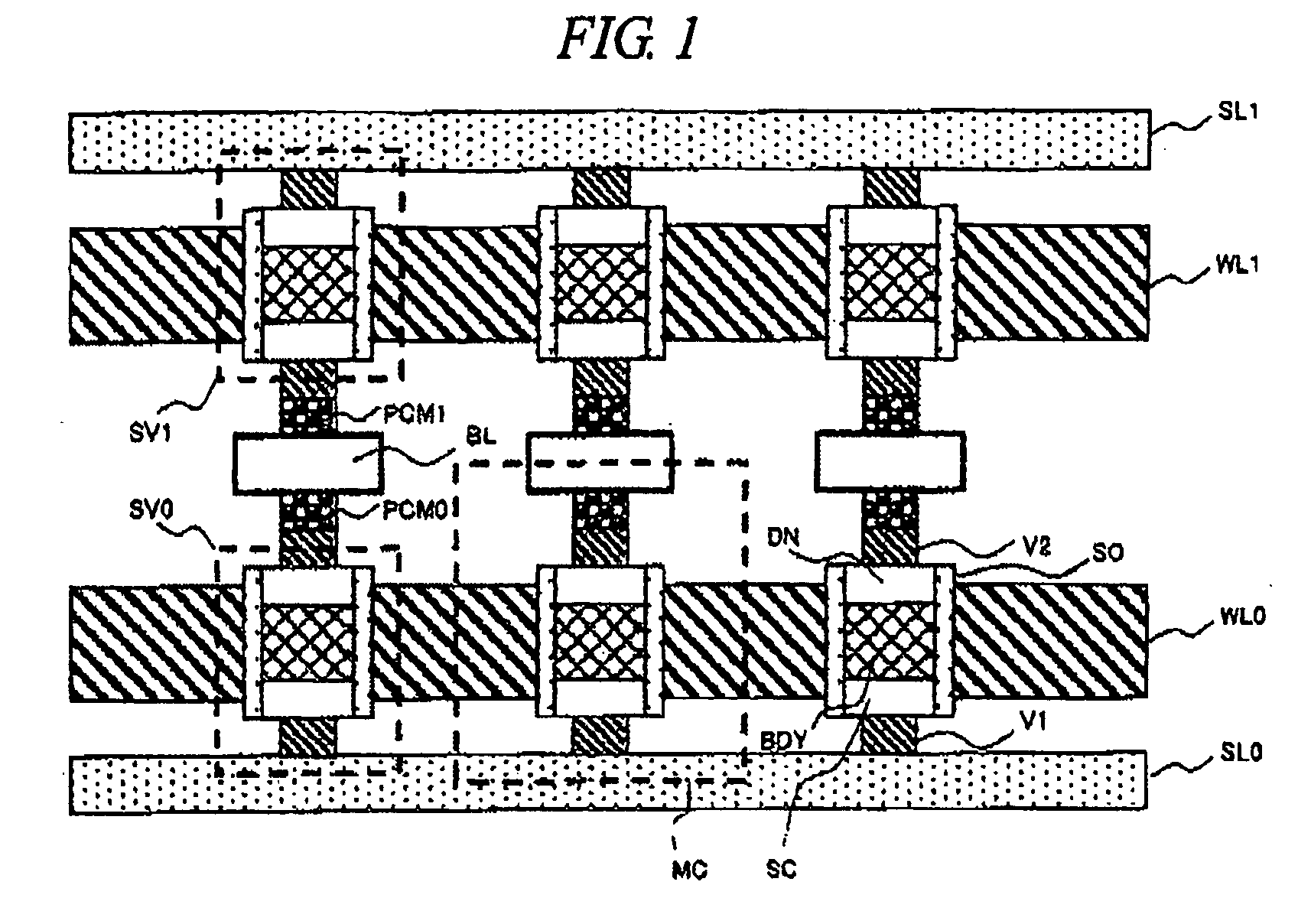
[0059] The vertical transistor referred to in Embodiment 1 is left floating since no electricity is fed to the channel part BDY. Therefore, the electric potential is unstable, and the history effect in which the threshold of the transistor is varied becomes a problem. Therefore, an example in which electricity is fed to the channel part of a transistor will be explained.
[0060]FIG. 13 shows a plan view of a memory array of the present embodiment. The shown memory array has two cells in the direction of word lines WL, and two cells in the direction of bit lines BL. A memory cell MC comprising a vertical transistor and a memory element is disposed on the intersecting point of the word line WL and the bit line BL. The bit line BL is disposed with a pitch of 4F, and the word line WL is disposed with a pitch of 2F, therefore, the area of a memory cell becomes 8F2 which is double comparing with that in Embodiment 1. The cross section taken from B-B' of the plan view is shown...
embodiment 4
[Embodiment 4]
[0065] A case in which the memory block MB referred to in Embodiment 1 has a different structure is explained by using FIG. 19.
[0066] The memory array of a memory block MBc is separated into two memory arrays (ARRAYl and ARRAYr). Each array comprises plural word lines and plural bit lines, and memory cells are connected at the intersecting points of the word lines and the bit lines. Each memory cell comprises a vertical N-channel type MOS transistor and a memory element. The memory element is, for example, an element called phase-change resistor.
[0067] Word driver circuits (WD0 and WDn) are connected to the word lines (WL0 and WLn). The word driver circuits (WD0 and WDn) are disposed in an array to form a word driver block WDB.
[0068] Dummy arrays (DUMMYl and DUMMYr) are disposed on the both sides of the memory arrays (ARRAYl and ARRAYr). Each of the dummy arrays (DUMMYl and DUMMYr) is comprised of two columns. One column comprises dummy cells (MDr0 , . . ., MDrn), a...
PUM
 Abstract
Description
Claims
Application Information