Multi-layer stacks for 3D NAND extendability

a multi-layer stack and extendability technology, applied in the direction of semiconductor devices, electrical equipment, basic electric elements, etc., can solve the problems of layer thickness, high aspect ratio etching, and oxide quality (i.e. breakdown voltage), and achieve the effect of reducing the thickness of the layer, and improving the etching

Active Publication Date: 2019-04-18
APPLIED MATERIALS INC
View PDF0 Cites 5 Cited by
  • Summary
  • Abstract
  • Description
  • Claims
  • Application Information

AI Technical Summary

Benefits of technology

[0003]The designs of memory and other semiconductor devices have undergone rapid development in recent years. Current memory devices are able to retain stored data for a very long period of time without applying a voltage thereto, and the reading rate of such memory devices is relatively high. It is relatively easy to erase stored data and rewrite data into the memory devices. Thus, memory devices have been widely used in micro-computers, and automatic control systems, etc. To increase the bit density and reduce the cost per bit of memory devices, 3D NAND (three-dimensional Not AND) memory devices have been developed. Other memory devices, such as ReRAM (resistive random access memory), and advanced hardmask materials are also being developed to further facilitate advances in the semiconductor industry.
[0004]Vertical gate 3D memory cells are being explored for 3D NAND technologies to reduce cost as the number of memory cell layers increase. Oxide / silicon and oxide / nitride layer stacks are useful due to material integration advantages, but with an increasing number of memory cell layers, thickness of the layers becomes a limiting factor. Thus, reducing the thickness of the memory cell layers is desirable, however, issues of oxide quality (i.e. breakdown voltage), silicon resistivity, and high aspect ratio etching persist with reduced layer thickness.

Problems solved by technology

Oxide / silicon and oxide / nitride layer stacks are useful due to material integration advantages, but with an increasing number of memory cell layers, thickness of the layers becomes a limiting factor.
Thus, reducing the thickness of the memory cell layers is desirable, however, issues of oxide quality (i.e. breakdown voltage), silicon resistivity, and high aspect ratio etching persist with reduced layer thickness.

Method used


Image

  • Multi-layer stacks for 3D NAND extendability
  • Multi-layer stacks for 3D NAND extendability
  • Multi-layer stacks for 3D NAND extendability

Examples


Embodiment Construction

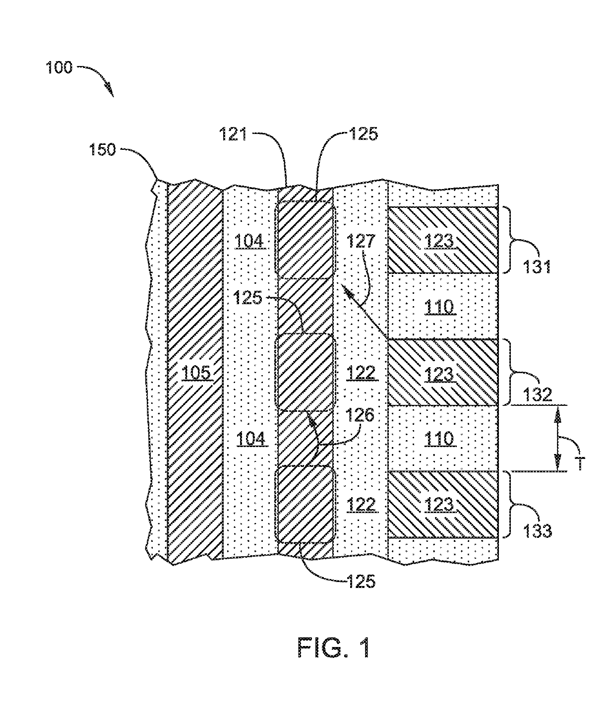
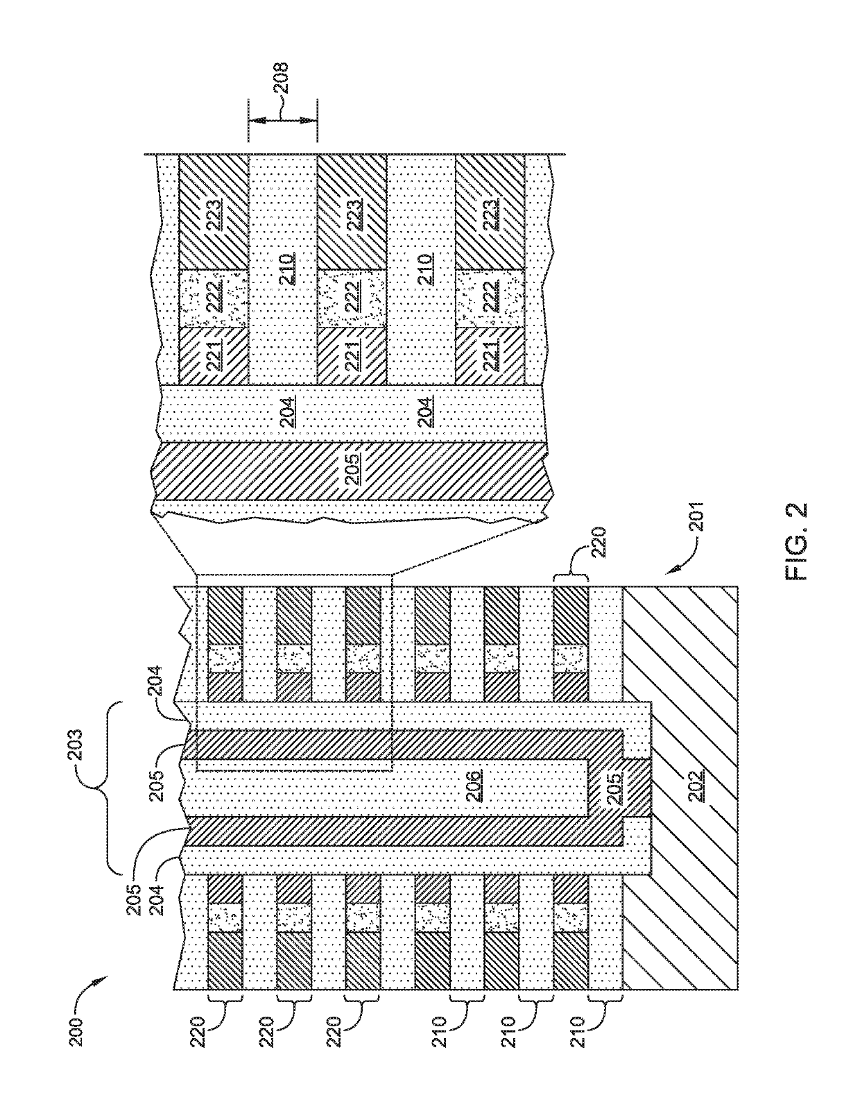
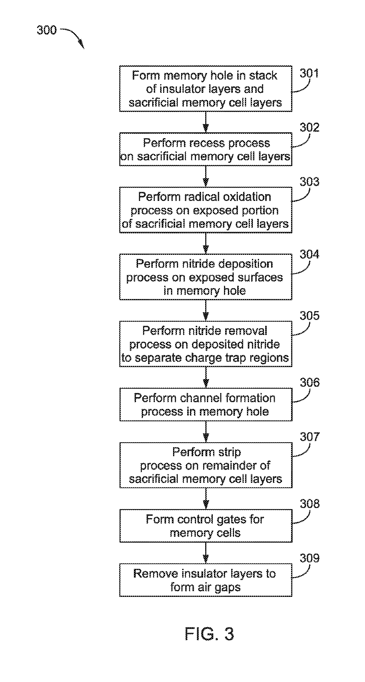
[0017]Embodiments described herein relate to methods and materials for fabricating semiconductor devices, such as memory devices and the like. In one embodiment, a memory layer stack includes materials having differing etch rates in which one material is selectively removed to form an airgap in the device structure. In another embodiment, silicon containing materials of a memory layer stack are doped or fabricated as a silicide material to reduce sheet resistance of the silicon containing material. In another embodiment, a silicon nitride material is utilized as an interfacial layer between oxide containing and silicon containing layers of a memory layer stack to improve adhesion between the oxide and silicon containing layers.

[0018]In a conventional three-dimensional (3D) NAND memory device, the charge storage region of a memory cell may be susceptible to leakage of trapped charge into or out of the charge storage region of adjacent memory cells, compromising stored data, as illust...


PUM

PropertyMeasurementUnit
thicknessaaaaaaaaaa
thicknessaaaaaaaaaa
diameteraaaaaaaaaa

Abstract

Embodiments described herein relate to methods and materials for fabricating semiconductor devices, such as memory devices and the like. In one embodiment, a memory layer stack includes materials having differing etch rates in which one material is selectively removed to form an airgap in the device structure. In another embodiment, silicon containing materials of a memory layer stack are doped or fabricated as a silicide material. In another embodiment, a silicon nitride material is utilized as an interfacial layer between oxide containing and silicon containing layers of a memory layer stack.

Description

CROSS-REFERENCE TO RELATED APPLICATIONS[0001]This application claims benefit to U.S. Provisional Patent Application No. 62 / 571,565, filed Oct. 12, 2017, the entirety of which is herein incorporated by reference.BACKGROUNDField[0002]Embodiments of the present disclosure generally relate to methods and materials for forming semiconductor devices. More specifically, embodiments described herein relate to multi-layer stacks for three dimensional (3D) not AND (NAND) extendibility.Description of the Related Art[0003]The designs of memory and other semiconductor devices have undergone rapid development in recent years. Current memory devices are able to retain stored data for a very long period of time without applying a voltage thereto, and the reading rate of such memory devices is relatively high. It is relatively easy to erase stored data and rewrite data into the memory devices. Thus, memory devices have been widely used in micro-computers, and automatic control systems, etc. To incre...

Claims


Application Information

Patent Timeline
Patent Type & Authority Applications(United States)
IPC IPC(8): H01L27/11582H01L27/1157H01L21/02
CPCH01L27/11582H01L27/1157H01L21/02164H01L21/31116H10B43/35H10B43/27H01L21/7682H01L21/76832H10B41/35H10B41/27
Inventor HAN, XINHAIPADHI, DEENESHPING, ER-XUANGUGGILLA, SRINIVAS
Owner APPLIED MATERIALS INC
Why Eureka
Try Eureka