Semiconductor memory device

a memory device and semiconductor technology, applied in the direction of read-only memories, semiconductor devices, instruments, etc., can solve the problems of high cost, large area, and relatively long manufacturing steps, and achieve the effects of small area, simple equipment, and reduced manufacturing steps

Active Publication Date: 2011-06-09
SEMICON ENERGY LAB CO LTD
View PDF99 Cites 19 Cited by
  • Summary
  • Abstract
  • Description
  • Claims
  • Application Information

AI Technical Summary

Benefits of technology

[0062]By the present invention, effects such as the following can be expected. Firstly, writing can be done faster than MROM in which a contact is formed by a photolithography step, and area reduction can be expected. Writing is possible in a simple step, because data can be written by irradiating with ultraviolet light a desired portion of a substrate including an oxide semiconductor in an active layer, using simple equipment. Secondly, although a photoresist step utilizing a photomask is performed for writing when manufacturing MROM, manufacturing according to the present invention utilizing ultraviolet light is inexpensive. Thirdly, additional data wiring is possible during use. Fourthly, because one-time erasure of data is ultimately possible, when an IC chip using the present invention is destroyed, there is no case of it being disposed of while wri

Problems solved by technology

However, even when the mask ROM method is used to form a memory device, manufacturing steps are relatively complex, and in many cases, the cost is high.
That is, it is necessary to perform a step for manufacturing a photomask, which is a step that requires an expensive apparatus and a step with poor throughput that requires extremely long processing time.
There is also a method using a laser, but this also required complex steps and an expensive apparatus.
Also, in both methods of the mask ROM method and the organic memory, not only is there a problem during manufacturing of the identification number for every IC chip, after it is us

Method used


Image

  • Semiconductor memory device
  • Semiconductor memory device
  • Semiconductor memory device

Examples


embodiment 1

[0087]In this embodiment, a semiconductor memory device which is an embodiment of the present invention is described.

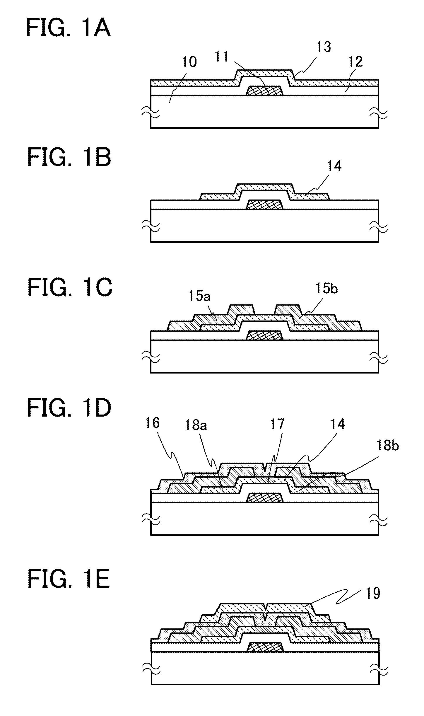
[0088]To describe using a thin film transistor is FIGS. 1A to 1E, a gate electrode layer 11 is formed over a substrate with an insulating surface, and then a gate insulating layer 12 is formed thereover. Then, an oxide semiconductor layer 14 is formed thereover, and a source electrode layer 15a and a drain electrode layer 15b are formed over a source portion and a drain portion of the oxide semiconductor layer, respectively. Next, after forming an oxide insulating layer 16, a back gate electrode layer 19 is formed. That is, over a surface of the semiconductor layer that is opposite the side on which the gate insulating layer and the gate electrode layer are formed, an oxide insulating layer and a back gate electrode layer are formed. As opposed to the gate electrode layer applying an electrical field to the semiconductor layer and controlling switching of the semicond...

embodiment 2

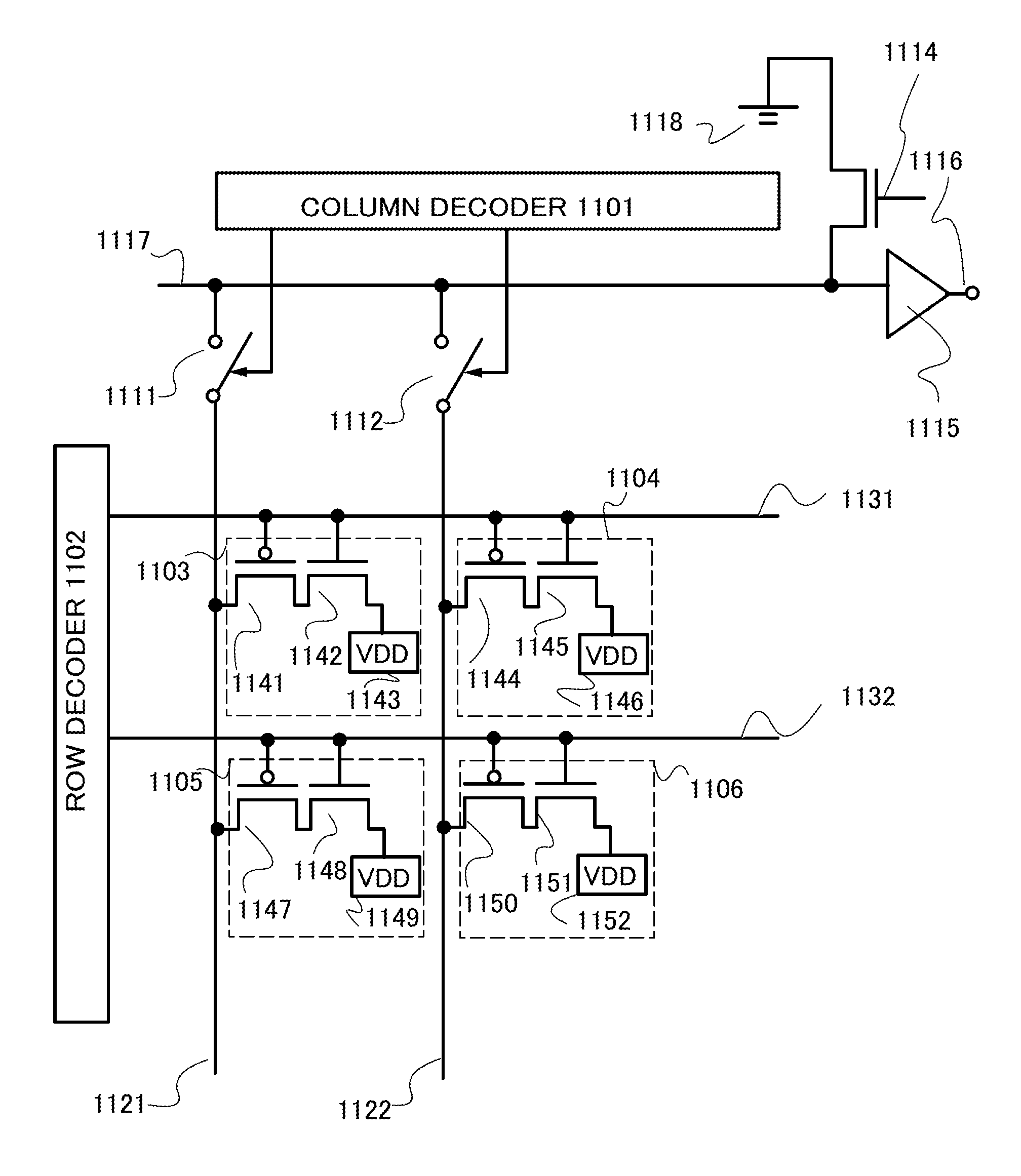
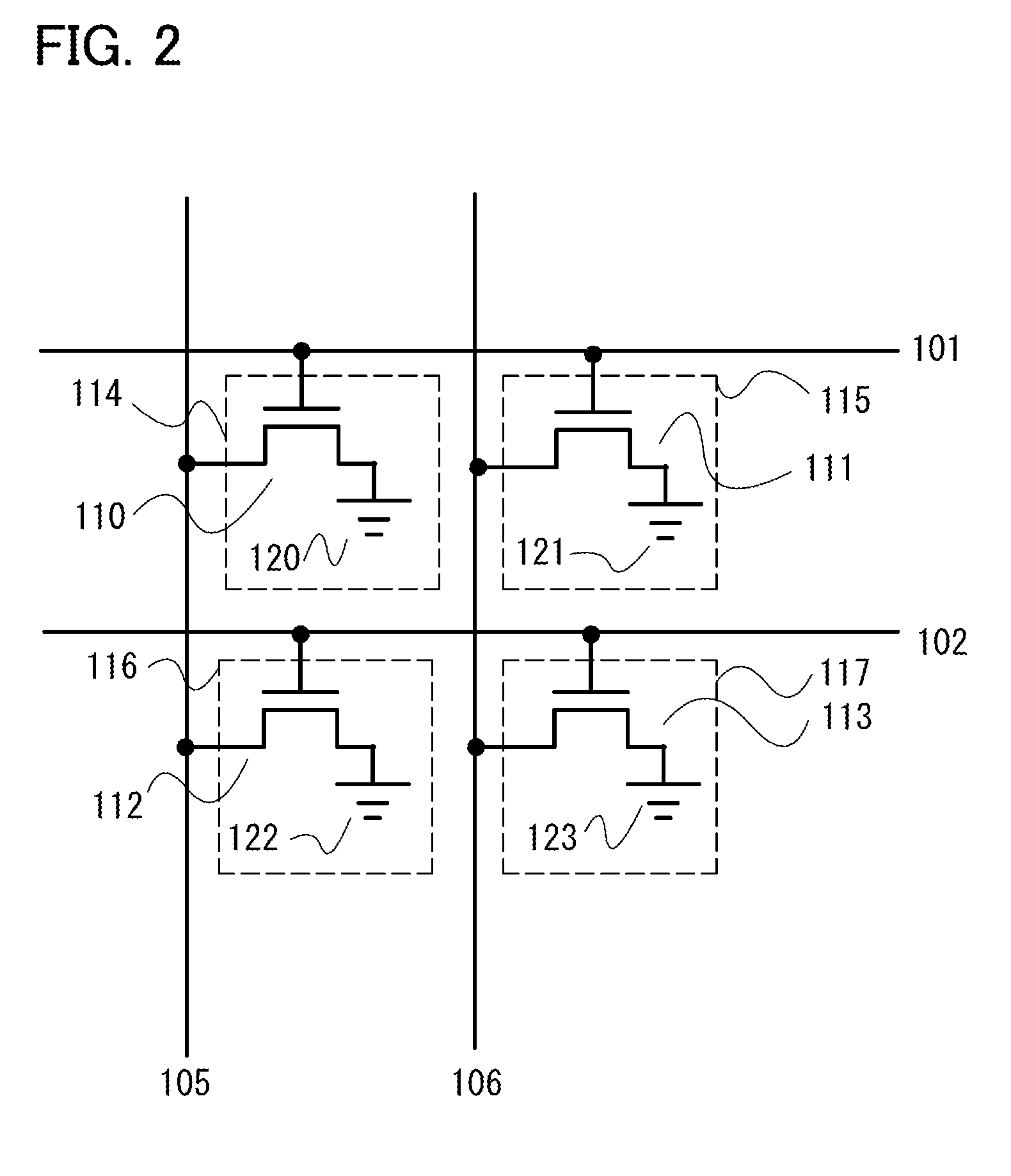
[0166]An embodiment in which another thin film transistor is provided inside a bit in addition to a thin film transistor including an oxide semiconductor will be explained. If the thin film transistor including an oxide semiconductor has an n-channel type electrical characteristic, a thin film transistor with a p-channel type electrical characteristic is used, which is the opposite polarity. With the p-channel type electrical characteristic, small current flows between a source and a drain when a positive voltage is applied to a gate electrode layer and large current flows when a negative voltage is applied. That is, it has a switching characteristic, by which an OFF state is obtained when a positive voltage is applied and an ON state is obtained when a negative voltage is applied. Furthermore, the n-channel thin film transistor has the opposite operation where an OFF state is obtained with a negative voltage and an ON state is obtained with a positive voltage. If the thin film tran...

embodiment 3

[0214]This embodiment describes a memory module 1500 to which one of the embodiments 1 and 2 is applied (see FIG. 15). The memory module 1500 includes a first memory cell region 1501, an interface 1503, a row decoder 1504, and a column decoder 1506.

[0215]In the first memory cell region 1501, a plurality of memory cell arrays described in the above embodiments is provided. In a second memory cell region 1502, a plurality of memory cell arrays described in the above embodiments is provided (see FIG. 15).

[0216]The row decoder 1504 corresponds to the row decoder 602 shown in Embodiment 1, for example, and is connected to the first memory cell region 1501 by a word line 1507.

[0217]The column decoder 1506 corresponds to the column decoder 601 shown in Embodiment 1, for example, and has a readout circuit and is connected to the first memory cell region 1501 and the second memory cell region 1502 by a bit line 1509.

[0218]Each of the row decoder 1504, the row decoder 1505, and the column dec...


PUM


Abstract

To provide a semiconductor memory device including an oxide semiconductor that can deal with instability of a threshold characteristic, in which writing is possible by a simple method. The semiconductor memory device functions by utilizing a characteristic that a threshold shifts when a thin film transistor including an oxide semiconductor is irradiated with ultraviolet light. Readout can be performed by setting a readout voltage between the threshold before the ultraviolet light irradiation and the threshold after irradiation. The threshold characteristic of an initial characteristic can be controlled by providing a back gate or by using two thin film transistors.

Description

BACKGROUND OF THE INVENTION[0001]1. Field of the Invention[0002]The present invention relates to a semiconductor memory circuit.[0003]2. Description of the Related Art[0004]A technique of forming a thin film transistor (TFT) by using a semiconductor thin film formed over a substrate with an insulating surface has attracted attention. Thin film transistors have been used in display devices typified by liquid crystal televisions. Silicon-based semiconductor materials such as amorphous silicon and low temperature crystallized silicon are known as materials for semiconductor thin films that can be applied to thin film transistors, and as another material, an oxide semiconductor has also attracted attention.[0005]As a material for the oxide semiconductor, zinc oxide or a material containing zinc oxide as a component are known. Also, a thin film transistor made of an amorphous oxide (an oxide semiconductor) with an electron carrier concentration of lower than 1018 / cm3 is disclosed (see Pa...

Claims


Application Information

Patent Timeline
IPC IPC(8): G11C17/12
CPCG11C17/12G11C17/18H01L27/1052H01L27/1214H01L27/105H01L27/1225H01L27/1288H10B99/00
Inventor SAITO, TOSHIHIKO
Owner SEMICON ENERGY LAB CO LTD
Why Eureka
Try Eureka