Semiconductor integrated circuit and method for testing the same

a technology of integrated circuits and semiconductors, applied in the direction of pulse techniques, instruments, transmission monitoring, etc., can solve the problems of inability to execute tests, inconvenient mass production methods, and no clock signals having a frequency difference can be generated

Inactive Publication Date: 2005-09-15
KK TOSHIBA
View PDF7 Cites 29 Cited by
  • Summary
  • Abstract
  • Description
  • Claims
  • Application Information

AI Technical Summary

Problems solved by technology

For this reason, no clock signals having a frequency difference can be generated, and the test cannot be executed.
However, this test method is not suitable for mass production because it is time-consuming, and it is difficult to control the fre...

Method used


Image

  • Semiconductor integrated circuit and method for testing the same
  • Semiconductor integrated circuit and method for testing the same
  • Semiconductor integrated circuit and method for testing the same

Examples


first embodiment

(1) First Embodiment

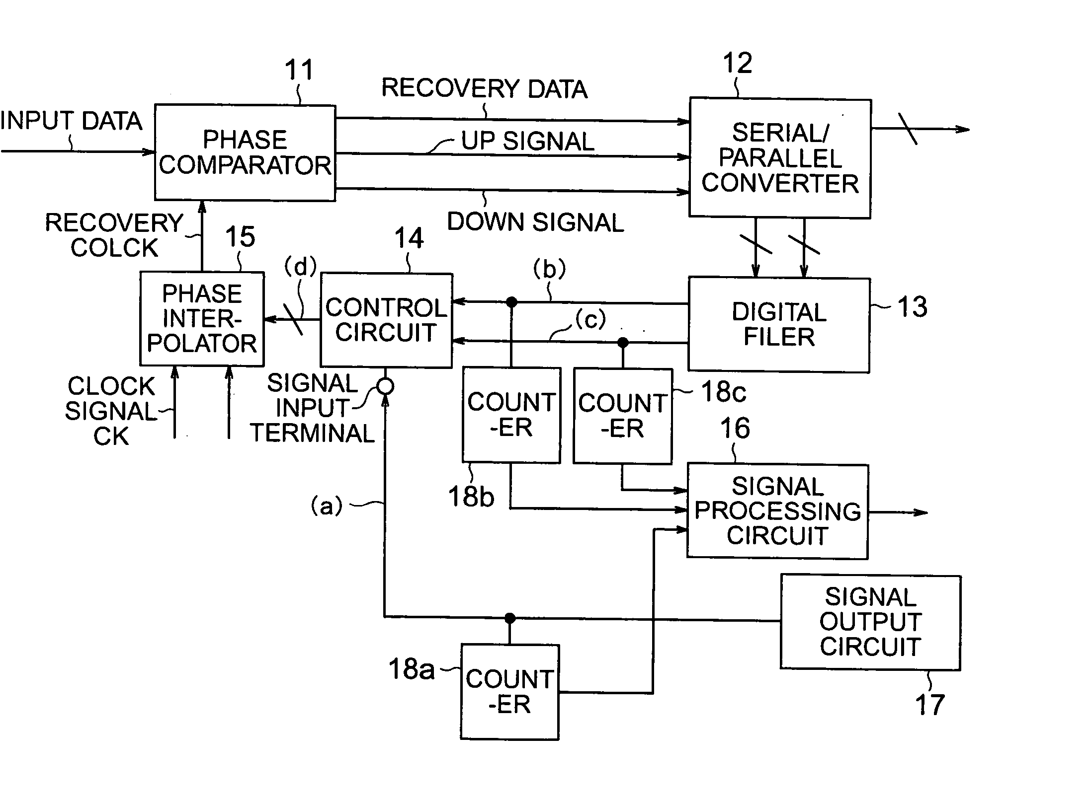
[0065]FIG. 1 shows the arrangement of a CDR circuit included in the receiver in a semiconductor integrated circuit according to the first embodiment of the present invention. The arrangement of the transmitter / receiver is the same as that shown in FIG. 6. In a loop back test, a test signal output from a transmitter 50 is input to a receiver 51, as shown in FIG. 9.

[0066] The CDR circuit comprises a signal processing circuit 16, signal output circuit 17, and counters 18a, 18b, and 18c in addition to a phase comparator 11, serial / parallel converter 12, digital filer 13, control circuit 14, and phase interpolator 15.

[0067] The operations of the phase comparator 11, serial / parallel converter 12, digital filer 13, control circuit 14, and phase interpolator 15 are the same as those of the circuits shown in FIG. 7, and a description thereof will be omitted.

[0068] The signal output circuit 17 inputs a signal having a predetermined frequency difference necessary for the...

second embodiment

(2) Second Embodiment

[0092]FIG. 4 shows the circuit arrangement of the second embodiment of the present invention.

[0093] In the first embodiment, the signal output circuit 17 supplies the signal (a) corresponding to a specific frequency difference to the control circuit 14.

[0094] The second embodiment is different from the first embodiment in that a signal output circuit 17 supplies a generated signal (a) to a digital filer 13. The same reference numerals as in the first embodiment denote the same elements in the second embodiment, and a description thereof will be omitted.

[0095] Even in the second embodiment, the frequency difference absorbing capability of the CDR circuit can easily be verified by executing a loop back test, as in the first embodiment.

third embodiment

(3) Third Embodiment

[0096]FIG. 5 shows the circuit arrangement of the third embodiment of the present invention.

[0097] In the third embodiment, a data error detector 19 is added to the arrangement of the first embodiment.

[0098] The data error detector 19 is connected to the output terminal of a serial / parallel converter 12 and the input terminal of a signal processing circuit 16. The data error detector 19 receives recovery data output from the serial / parallel converter 12, compares the recovery data with input data, and outputs the comparison result to the signal processing circuit 16.

[0099] According to the third embodiment, by using both the determination result from the signal processing circuit 16 and the comparison result output from the data error detector 19, the frequency difference absorbing capability of the CDR circuit can more accurately be verified, as in the first embodiment.

[0100] As described above, according to the semiconductor integrated circuits according to...


PUM


Abstract

According to the present invention, there is provided a semiconductor integrated circuit having a receiver which receives reception data and executes reception processing on the basis of a clock signal supplied from a PLL and a transmitter which receives parallel transmission data and executes serial transmission processing on the basis of the clock signal, and having a loop back function of supplying data output from the transmitter to the receiver for test, the receiver, as a CDR circuit, executing control so as to make the phase of the input data coincide with that of the recovery clock by a negative feedback loop having a phase comparator which receives input data and a recovery clock, compares a phase of the input data with that of the recovery clock, and outputs recovery data and a phase comparison result in a serial form, a serial/parallel conversion circuit which receives the phase comparison result, or the phase comparison result and the recovery data from the phase comparator, executes serial/parallel conversion, and outputs the phase comparison result in a parallel form, a digital filer which receives the phase comparison result from the serial/parallel conversion circuit, executes averaging processing for the phase comparison result in a predetermined period, and outputs the phase comparison result, a control circuit which receives the phase comparison result from the digital filer and outputs a control signal to control the phase of the recovery clock, and a phase interpolator which receives the clock signal and generates the recovery clock on the basis of the control signal, and the CDR circuit including a signal output circuit which inputs, to one of the control circuit and the digital filer, a signal to forcibly shift the phase of the recovery data in the negative feedback loop by a predetermined amount, a first counter which counts the number of pulses of the signal output from the signal output circuit in a predetermined period and outputs a first count value, a second counter which counts the number of pulses of the phase comparison result, which has undergone the averaging processing and is output from the digital filer, and outputs a second count value, and a signal processing circuit which receives the first count value and the second count value and compares the first count value with the second count value to determine presence/absence of a capability for absorbing the phase shift generated by the signal.

Description

CROSS REFERENCE TO RELATED APPLICATION [0001] This application is based upon and claims benefit of priority under 35 USC §119 from the Japanese Patent Application No. 2004-67206, filed on Mar. 10, 2004, the entire contents of which are incorporated herein by reference. BACKGROUND OF THE INVENTION [0002] The present invention relates to a semiconductor integrated circuit and a method for testing the same and, more particularly, to a semiconductor integrated circuit and a test method which are suitable for a GHz-class high-speed I / O interface. [0003] Along with the recent increase in speed of the input / output interface of a semiconductor integrated circuit, a demand has arisen for processing signals in a GHz band. [0004]FIG. 6 shows the arrangement of a transmitter (TX) 50, receiver (RX) 51, and PLL (Phase Locked Loop) 52 used in an input interface. [0005] The transmitter 50 receives low-speed parallel transmission data, converts the data into high-speed serial data, and outputs the c...

Claims


Application Information

Patent Timeline
IPC IPC(8): G01R31/317G01R31/28H01L21/822H01L27/04H03K5/26H04B1/10H04L7/033
CPCG01R31/31716
Inventor SHIZUKI, YASUSHI
Owner KK TOSHIBA
Why Eureka
Try Eureka