Multiple Electrical Level Dispersion Tolerant Optical Apparatus

a technology of optical apparatus and electrical level, applied in the direction of electrical apparatus, electromagnetic transmission, electromagnetic transmission, etc., can solve the problems of inconvenient use, high cost, and bulky, and achieve the effect of simple and less costly, low cost of implementing nrz or rz modulation schemes, and easy availability of components

Inactive Publication Date: 2009-02-19
HONG JIN +1
View PDF0 Cites 31 Cited by
  • Summary
  • Abstract
  • Description
  • Claims
  • Application Information

AI Technical Summary

Benefits of technology

[0014]An advantage of the present invention applied to the receiver side, is that on the transmitter side, most of the conventional and widely used intensity modulation schemes can still be practically used without need of modifications, such as the use of non-return-to-zero (NRZ) modulation or return-to-zero (RZ) modulation schemes. The cost of implementing these conventional NRZ or RZ modulation schemes is low and the components are readily available. Compared with the conventional direct detection system for the demodulation of NRZ or RZ signals, the multi-level receiver design also needs only one photo detector at the receiving end. However, the key difference between them is the introduction of the electrical multi-level generation scheme after the photo detection and the implementation of multi-level parallel decision making circuits following that. Compared with the traditional balanced detection scheme, such as these used in the differential phase shift keying (DPSK) and quadrature phase shift keying (QPSK), or the differential quadrature phase shifted keying (DQPSK) systems, instead of utilizing the optical delay line interferometers at optical domain before photo detectors and two or more balanced photo-detectors for the demodulation of phase information contained in the incoming optical signals, current scheme utilizes the electrical delay line architecture right after a single photo detector in the electrical domain and parallel multiple electrical decision making circuitries for the direct detection of the incoming optical signals.
[0015]When the current invention is implemented on both the transmitter sid

Problems solved by technology

Optical fiber transmission systems are subject to distortion related to loss, noise, and nonlinearity in both the fiber and the modulation and amplification devices.
One of the more deleterious forms of signal distortion is that due to chromatic dispersion.
This type of approach is commonly used in the current commercial optical communication systems, but can be expensive, and bulky.
Due to the large insertion loss of optical compensation devices, there is a need for more amplifiers to compensate the loss of the devices, which is not only expensive to implement and significantly increase the system cost from material, space, power, and operation perspective, but also introduce more of the unnecessary amplifier noises which in fact reduce the optical signal to noise ratio (OSNR) of the transmission system, and therefore may either significantly degrade the receiver signal or reduce the total allowed transmission distance.
In the end, the cost of implementing these devices in the system is higher.
This type of coherent detection approach is expensive and only good for some applications.
It is not generic enough to cover most of the applications, especially for most of the practical low cost optical communication systems, where only the direct detection system is used in majority of the commercial systems.
This appro

Method used


Image

  • Multiple Electrical Level Dispersion Tolerant Optical Apparatus
  • Multiple Electrical Level Dispersion Tolerant Optical Apparatus
  • Multiple Electrical Level Dispersion Tolerant Optical Apparatus

Examples


Embodiment Construction

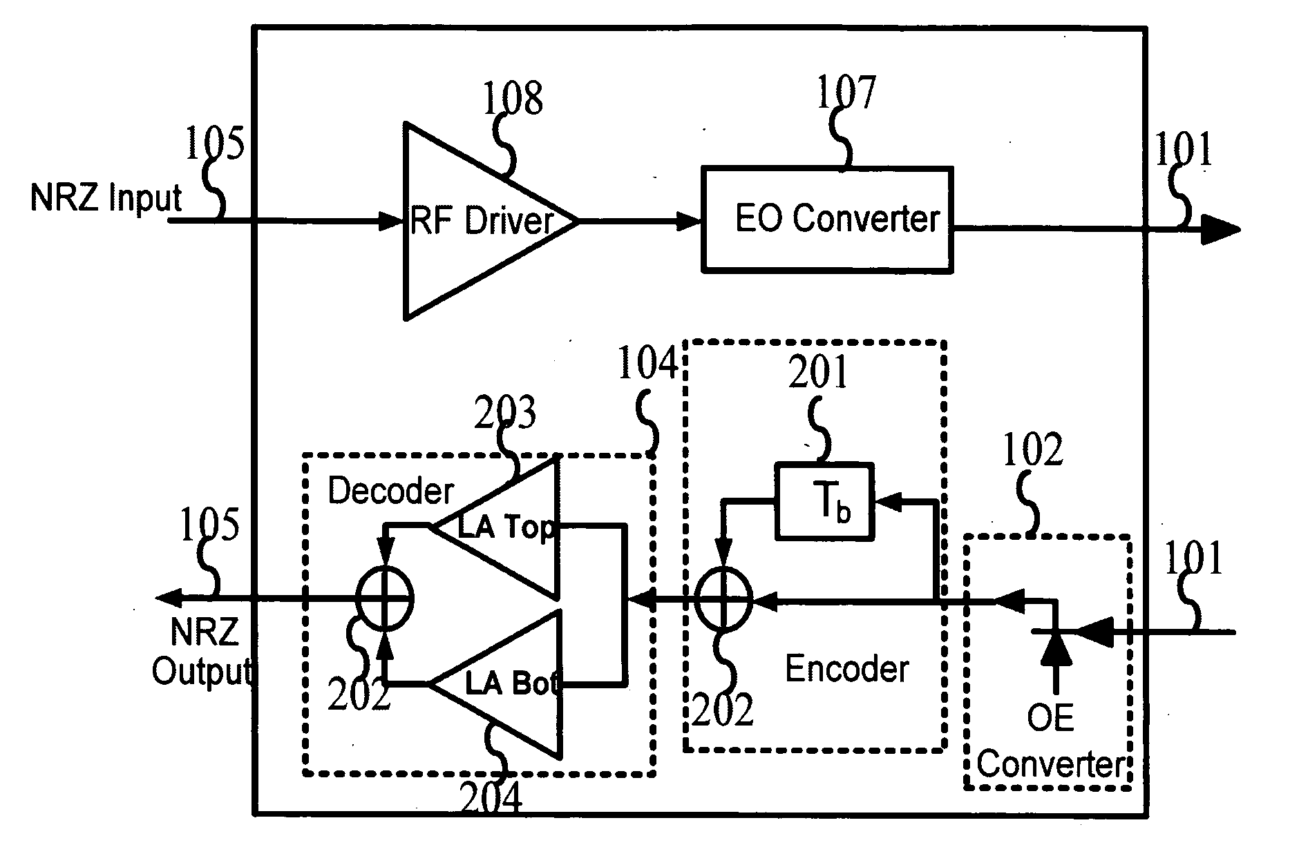
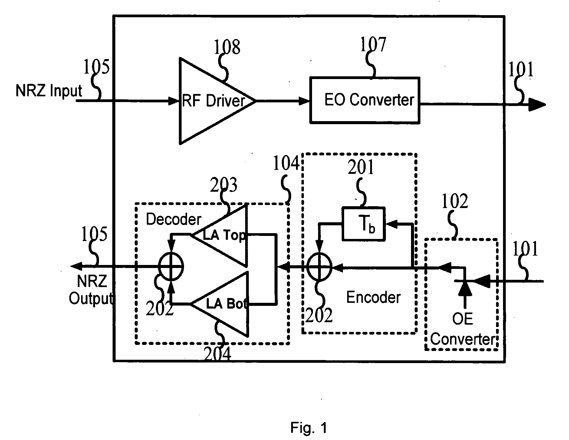
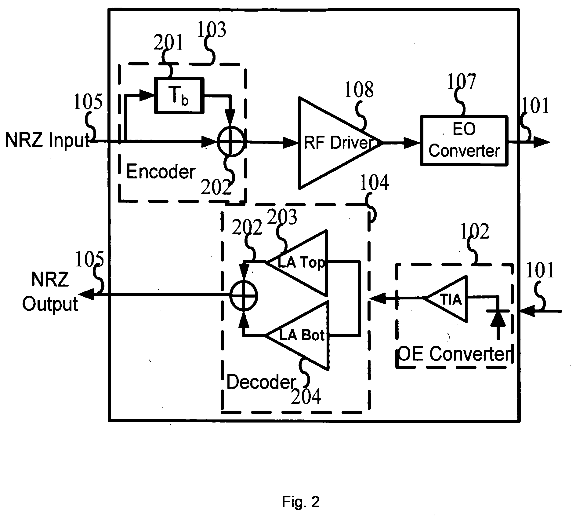
[0022]A transceiver according to an embodiment of the invention is shown in FIG. 1, where the present invention is implemented on the receiver side of the transmission system. The transceiver comprises a RF driver 108 and an electrical to optical convertor 107 on the transmitter chain. This transmitter chain is the typical implementation for NRZ system. The 107 block can be of other types of lasers and modulators to have the RZ, NRZ, Optical Single Side Band (OSSB) or Phase Shifted Binary Transmission (PSBT) modulation on the transmitter side. For example, the lasers can be the vertical cavity surface emitting lasers (VCSEL), or the FP lasers, or DFB lasers, or the external modulators can be of the MZ types, integrated, or hybrid integrated, or isolated from a CW laser. On the receiver chain, the received modulated light is firstly detected by a PIN or APD based photo detector 102 to perform the optical to electrical conversion. After that, the generated electrical signal is then fe...


PUM


Abstract

An optical apparatus consisting of a transmitter, receiver, or transceiver, utilizing a multiple level special electrical layer modulation and/or demodulation scheme to significantly lower the bandwidth required for high speed communication and/or parallel interconnect systems. It can be used either to enhance the transmission performance of the transceiver, or to eliminate the need for bulky and/or expensive optical components to lower the cost. It can be used in the design of transponders, transceivers, and active cabling systems, for 10 Gb/s, 40 Gb/s, 100 Gb/s and other high bit rate transmission systems that utilize single mode or multi-mode fibers for serial or parallel transmission of high speed optical signals.

Description

[0001]This U.S. application Ser. No. 12 / 132,616 is the official continuation filing of the previously filed provisional U.S. Patent Application No. 60 / 933,039, filed on Jun. 4, 2007, entitled “Dispersion tolerant electrical multi-level receivers and apparatus for low cost and high speed optical communications”, therefore claims the priority date of Jun. 4, 2007 of the provisional Patent Application U.S. 60 / 933,039, which is incorporated herein by reference.FIELD OF INVENTION[0002]The invention relates to the design of optical transmission systems, and in particular, to electrical multi-level transmitter and / or receiver design and apparatus using such design for the modulation and / or demodulation in the communication systems for high-speed low-cost serial or parallel applications.BACKGROUND OF THE INVENTION[0003]Optical fiber transmission systems are subject to distortion related to loss, noise, and nonlinearity in both the fiber and the modulation and amplification devices. One of t...

Claims


Application Information

Patent Timeline
IPC IPC(8): H04B10/00
CPCH04B10/40H04B10/541H04B10/695
Inventor HONG, JINSHANG, SONG
Owner HONG JIN
Why Eureka
Try Eureka