Process and system for laser crystallization processing of film regions on a substrate to provide substantial uniformity, and a structure of such film regions

Inactive Publication Date: 2005-09-15
IM JAMES S
View PDF96 Cites 63 Cited by
  • Summary
  • Abstract
  • Description
  • Claims
  • Application Information

AI Technical Summary

Benefits of technology

[0013] In another exemplary embodiment of the present invention, the first area has a first border and a second border which is provided opposite and parallel to the first border of the first area. Also, the second area has a third border and a fourth border which is provided opposite and parallel to the third border of the second area. A distance between the first border and the second border is smaller than a distance between the third border and the four

Problems solved by technology

Further, the uniformity in the thin film was found to be insensitive to a spatial non-uniformity of the beam incid

Method used


Image

  • Process and system for laser crystallization processing of film regions on a substrate to provide substantial uniformity, and a structure of such film regions
  • Process and system for laser crystallization processing of film regions on a substrate to provide substantial uniformity, and a structure of such film regions
  • Process and system for laser crystallization processing of film regions on a substrate to provide substantial uniformity, and a structure of such film regions

Examples


second embodiment

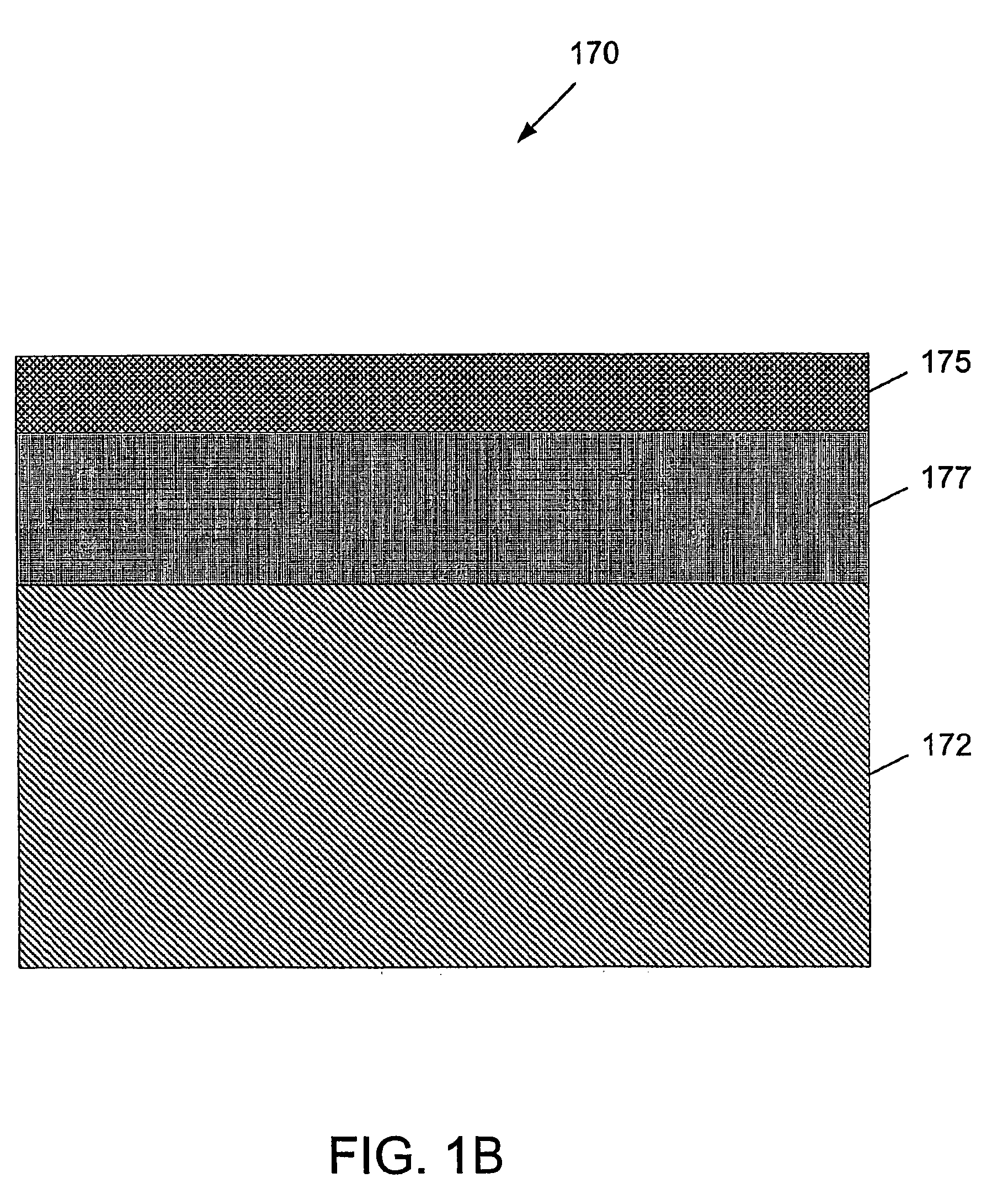
[0053]FIGS. 6A-6D show an exemplary progression of the process according to the present invention in which a plurality of successive areas along the first conceptual column 205 of the semiconductor thin film 175 is irradiated by the beam pulse 164 (comprised of beamlets) which is shaped by the mask 150′ of FIG. 5A. The translation of the sample 170 with sect to the impingement thereof by the beam pulse 164 is substantially the same as the translation described above with reference to FIGS. 4A-4F. The difference between the irradiation of the areas 310, 320, . . . , 380, 390, 410, 420 by the beam pulse 164 shaped by the mask 150 of FIG. 3 and the areas 460, 470 by the beam pulse 164 shaped by the mask 150′ is that substantially the entire areas 310, 320, . . . , 380, 390, 410, 420 are irradiated and completely melted, as opposed to only certain small portions 462 of the areas 460, 470 are irradiated and completely melted throughout their entire thickness.

[0054] Similarly to the area ...

third embodiment

[0055] In addition, it is possible to utilize a mask 150″ according to the present invention as shown in FIG. 7 which has a long and narrow open or transparent region 490 so as to pattern and shape the beam 149 into the beam pulse 164. For example, the length of the region 490 can be 0.5 cm and the width thereof may be 0.1 mm. In this manner, each conceptual column of the sample 170 illustrated in FIG. 2 can be irradiated by the beam pulse 164 shaped by this mask 150″. In addition, it may be possible for the length of the region 490 to be 30 cm. Thus, instead of subdividing the semiconductor thin film 175 into a number of conceptual columns, and irradiating each column separately, it is possible to irradiate and completely melt selected portions of the semiconductor thin film 175 by translating the sample 170 in the −Y direction from one edge of the sample 170 to the opposite edge thereof. It is important that the small-grained uniform regions be formed using such processing techniq...


PUM

PropertyMeasurementUnit
Thicknessaaaaaaaaaa
Structureaaaaaaaaaa
Sizeaaaaaaaaaa

Abstract

A process and system for processing a thin film sample (e.g., a semiconductor thin film), as well as the thin film structure are provided. In particular, a beam generator can be controlled to emit at least one beam pulse. With this beam pulse, at least one portion of the film sample is irradiated with sufficient intensity to fully melt such section of the sample throughout its thickness, and the beam pulse having a predetermined shape. This portion of the film sample is allowed to resolidify, and the re-solidified at least one portion is composed of a first area and a second area. Upon the re-solidification thereof, the first area includes large grains, and the second area has a region formed through nucleation. The first area surrounds the second area and has a grain structure which is different from a grain structure of the second area. The second area is configured to facilitate thereon an active region of an electronic device.

Description

RELATED APPLICATION [0001] This application claims priority to U.S. Provisional Application No. 60 / 405,084, which was filed on Aug. 19, 2002, and is incorporated by reference.NOTICE OF GOVERNMENT RIGHTS [0002] The U.S. Government may have certain rights in this invention pursuant to the terms of the Defense Advanced Research Project Agency award number N66001-98-1-8913.FIELD OF THE INVENTION [0003] The present invention relates to techniques for processing of films, and more particularly to techniques for processing films to obtain a substantially uniform grain region for placing at least an active region of a thin-film transistor (“TFT”) therein. BACKGROUND OF THE INVENTION [0004] Semiconductor films, such as silicon films, are known to be used for providing pixels for liquid crystal display devices. Such films have previously been processed (i.e., irradiated by an excimer laser and then crystallized) via excimer laser annealing (“ELA”) methods. However, the semiconductor films pro...

Claims


Application Information

Patent Timeline
IPC IPC(8): C30B35/00H01L21/20H01L21/336H01L21/428H01L21/77H01L21/84H01L27/12H01L29/786
CPCH01L21/2026H01L27/1285H01L27/1296Y10T117/1076H01L29/78675Y10T117/1024H01L29/66757H01L21/02683H01L21/02686H01L21/02678H01L21/02422H01L21/02488H01L21/02532H01L21/02689H01L21/02691
Inventor IM, JAMES S.
Owner IM JAMES S
Why Eureka
Try Eureka