Photovoltaic conversion device, its manufacturing method and solar energy system

a technology of photovoltaic conversion and manufacturing method, which is applied in the direction of semiconductor devices, solid-state devices, pv power plants, etc., can solve the problems of reducing photovoltaic conversion efficiency, and achieve the effect of high photovoltaic conversion efficiency

Inactive Publication Date: 2005-09-22
KYOCERA CORP
View PDF3 Cites 12 Cited by
  • Summary
  • Abstract
  • Description
  • Claims
  • Application Information

AI Technical Summary

Benefits of technology

[0033] By using the photovoltaic conversion device having high photovoltaic conversion efficiency of the

Problems solved by technology

However, since the one conduction-type semiconductor particles are made to be exposed by grinding in the photovoltaic conversion device shown in FIG. 3, the grinding may lead to a defect such as a hole in the insulating layer 2 or peeling from

Method used


Image

  • Photovoltaic conversion device, its manufacturing method and solar energy system
  • Photovoltaic conversion device, its manufacturing method and solar energy system
  • Photovoltaic conversion device, its manufacturing method and solar energy system

Examples


examples

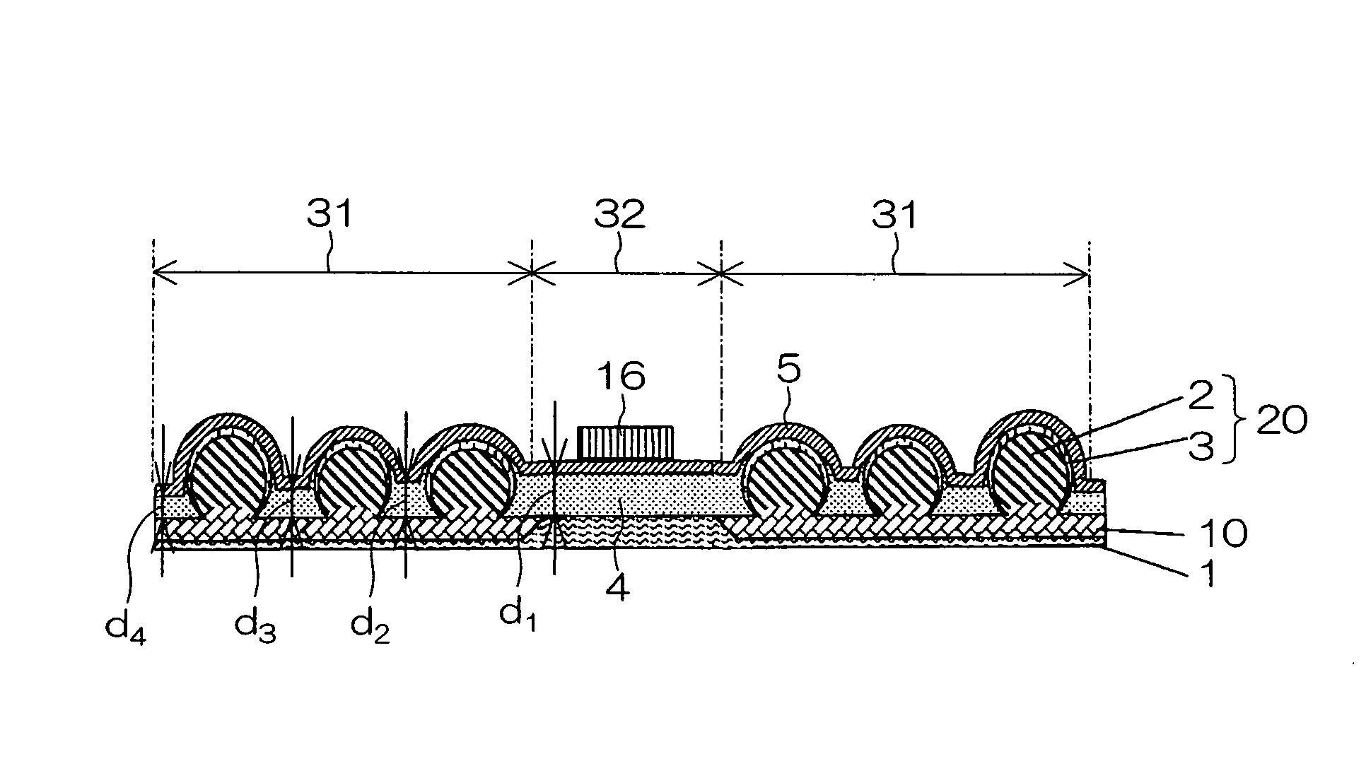
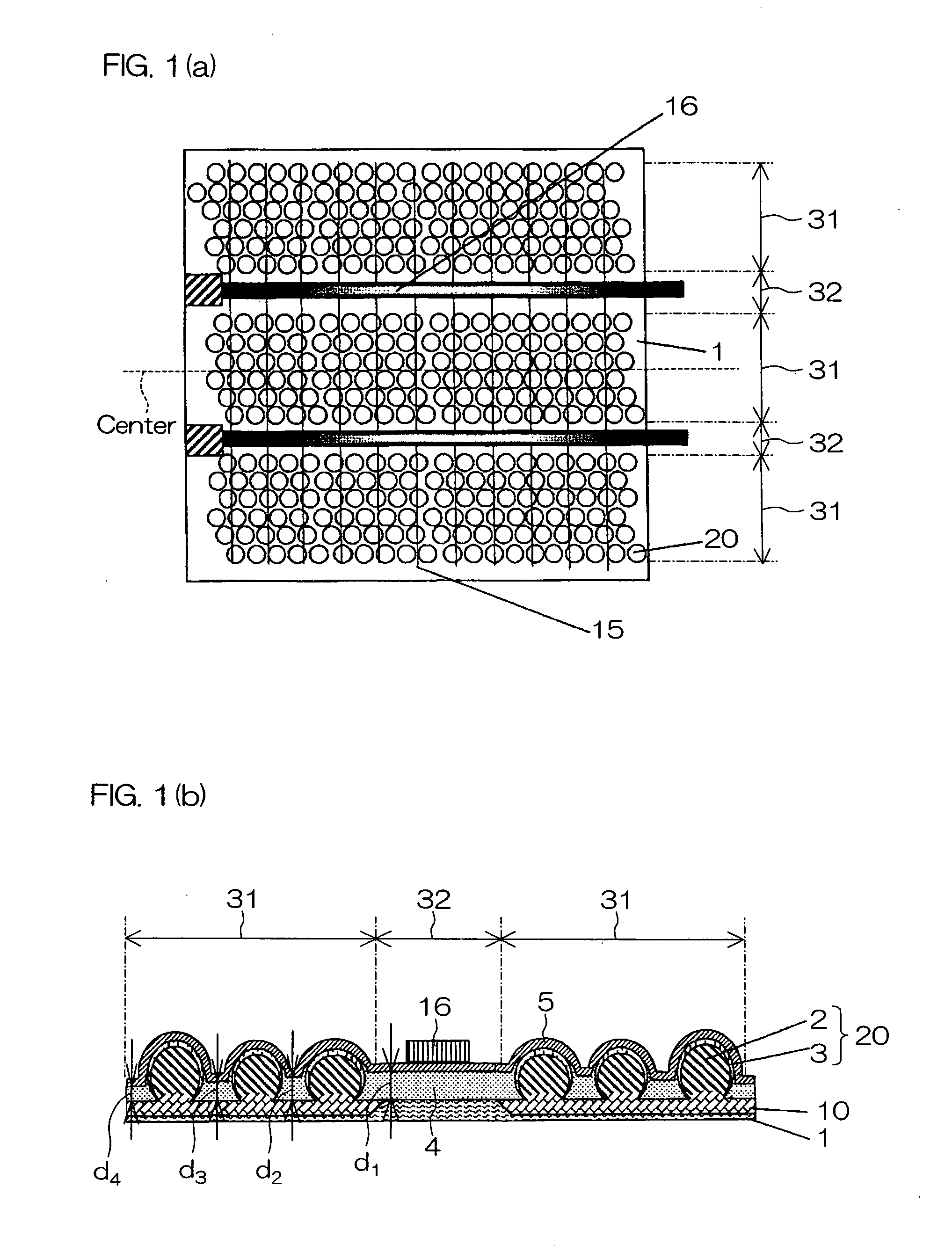
[0121] Next, a first example of the photovoltaic conversion device of the present invention will be described with reference to the photovoltaic conversion device shown in FIG. 1(a) and FIG. 1(b).

[0122] A lot of crystal semiconductor particles 2 as p-type silicon having a particle diameter ranging from 0.3 to 0.5 mm were placed on the substrate 1 made from aluminum in the first regions 31. Subsequently, the crystal semiconductor particles 2 were fixed by applying a certain amount of weight from above and heated in N2—H2 mixture atmosphere at 630° C. for 10 minutes in the fixed state. In this manner, the substrate 1 was joined to the crystal semiconductor particles 2 via the alloy layer 10 of the substrate 1 and the crystal semiconductor particles 2.

[0123] Subsequently, to clean the surface of the crystal semiconductor particles 2, the substrate 1 to which the crystal semiconductor particles 2 are joined was immersed in a mixed solution of hydrofluoric acid-nitric acid having a wei...


PUM


Abstract

A photovoltaic conversion device has a substrate 1 as a lower electrode having a first region 31 and a second region 32 adjacent to the first region, a lot of semiconductor particles 20 joined to the first region 31, an insulator 4 formed between the semiconductor particles 20 on the substrate 1 in the first region 31 and on the substrate 1 in the second region 32, a transparent conductive layer 5 as an upper electrode formed so as to cover the upper part of the semiconductor particles 20 in the first region 31 and the insulator 4 in the first region 31, and a collecting electrode formed of a finger electrode 15 arranged on the transparent conductive layer 5 in the first region 31 and a bus bar electrode 16 which is arranged in the second region 32 and connected to the finger electrode 15. By making the thickness of the insulator 4 in the second region 32 larger than that of the insulator 4 in the first region, even if generated photocurrents concentrate on the bus bar electrode 16, insulating properties between the substrate 1 and the transparent conductive layer 5 can be ensured stably, thereby to achieve high photovoltaic conversion efficiency.

Description

BACKGROUND OF THE INVENTION [0001] 1. Field of the Invention [0002] The present invention relates to a photovoltaic conversion device used for photovoltaic power generation and the like, its manufacturing method and a solar energy system. The present invention relates to, in particular, a photovoltaic conversion device using semiconductor particles, its manufacturing method and a solar energy system. [0003] 2. Description of Related Art [0004] An example of a conventionally proposed photovoltaic conversion device using semiconductor particles is shown in a sectional view of FIG. 3. [0005] As shown in FIG. 3, in the photovoltaic conversion device, a low-melting-point metal layer 108 is formed on a substrate 101 used as a lower electrode, a lot of one conduction-type semiconductor particles 103 are fixed to the low-melting-point metal layer 108 to be buried therein and an insulating layer 102 is formed so as to cover the fixed semiconductor particles 103 and the low-melting-point meta...

Claims


Application Information

Patent Timeline
IPC IPC(8): H01L25/00H01L31/04
CPCH01L31/022425H01L31/035281Y02E10/50H01L31/18H01L31/03529
Inventor OKUI, HIROKISEKI, YOJIMIURA, YOSHIOARIMUNE, HISAO
Owner KYOCERA CORP
Why Eureka
Try Eureka