
Structure for forming solar cells

Inactive Publication Date: 2015-06-11
INSTITUT NAT POLYTECHN DE GRENOBLE +1
View PDF5 Cites 1 Cited by
  • Summary
  • Abstract
  • Description
  • Claims
  • Application Information

AI Technical Summary

Benefits of technology

The present invention provides a structure made of a crystal silicon layer on a metal sheet for making low-cost solar cells that have a high photovoltaic conversion efficiency (>15%).

Problems solved by technology

The use of single-crystal silicon wafers provides the best efficiencies (maximum experimental efficiency 23%) but also results in extremely expensive products and such cells are practically only used when very high quality cells are necessary, for example, in satellites.
Above all, the different ingot conditioning operations (cropping, peeling) as well as the sawing of wafers result in a significant loss of material, of almost 50% of the ingot weight and of more than 50% of the initial silicon charge.
The deposition of a silicon layer on a conductive substrate, for example, metallic, is the less expensive solution but, in current techniques, this results in amorphous or microcrystallized silicon deposits.
In the case of microcrystallized silicon, the efficiency is in a higher range than that of amorphous silicon but is limited by a high defect rate with respect to crystal silicon.
Such defects are generated by a high density of grain boundaries and by the accumulation of defects (dislocations, point defects, impurities .
Thus, current solar cell substrate manufacturing methods have various disadvantages in terms of compromise between cost and efficiency.
Further, the forming of crystal silicon at temperatures lower than 800° C. provides a material having a high rate of structural defects, which adversely affects the conversion efficiency and limits the growth speed.
The formed material thus has the same disadvantages as that previously described, that is, a high rate of structural defects and a very low growth speed.
In such a method, the substrate can thus not play an active role in the photovoltaic cell and only forms a mechanical support for the deposited silicon.

Method used


Image

  • Structure for forming solar cells
  • Structure for forming solar cells

Examples


Embodiment Construction

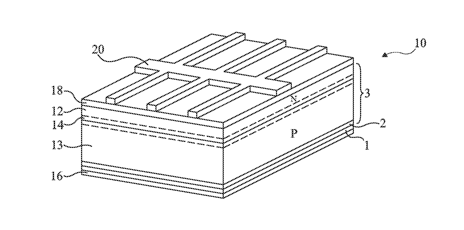
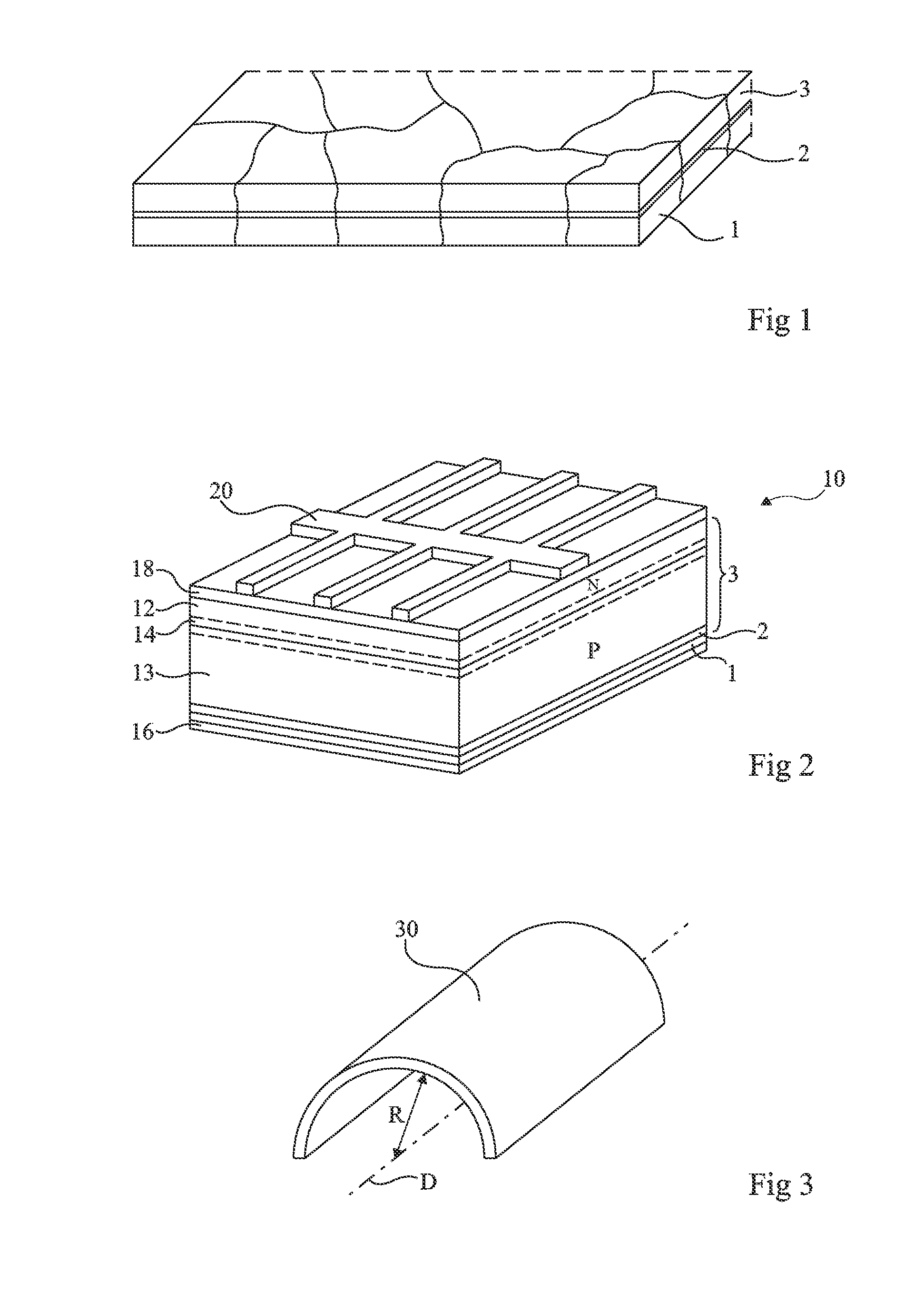
[0036]As illustrated in FIG. 1, a structure adapted to the forming of solar cells according to an embodiment of the present invention comprises, on a metal support 1, an electrically-conductive bather layer 2 and a multicrystal silicon layer, preferably doped as an electron acceptor (type P) 3.

[0037]Support 1 is a metal sheet having a sufficient thickness to ensure its mechanical hold, for example, a thickness greater than 100 μm. This sheet is formed from a structured metal, that is, a metal having crystal grains of relatively large dimension, for example, crystal grains having an average dimension greater than 50 μm, which may reach values ranging from 1 to 5 mm. An example of such a metal sheet is a stainless steel sheet, for example comprising a percentage of chromium approximately ranging from 15 to 25%. Such a product is commonly available for sale. The upper surface of this metal sheet is processed to be surface-deoxidized, for example, by a treatment with one or several acid...


PUM

PropertyMeasurementUnit
Temperatureaaaaaaaaaa
Lengthaaaaaaaaaa
Lengthaaaaaaaaaa

Abstract

The invention relates to a structure adapted for the formation of solar cells, comprising the following successive elements, namely: a sheet (1) of textured metal with crystal grains having an average size greater than 50 μm, said sheet being adapted to form a rear face electrode of the cells; a diffusion barrier layer (2) having a thickness of between 0.2 and 2 μm, made from an electrically conductive material with crystal grains having an average size greater than 50 μm; and a doped multicrystalline silicon layer (3) having a thickness of between 30 and 100 μm, with crystal grains having an average size greater than 50 to 100 μm, in which the average diffusion length of the carriers is greater than 50 μm.

Description

CROSS-REFERENCE TO RELATED APPLICATIONS[0001]The present application is a National Stage of PCT International Application Ser. No. PCT / FR2012 / 050195, filed Jan. 30, 2012, which claims priority under 35 U.S.C. §119 of French Patent Application Ser. No. 11 / 50718, filed Jan. 31, 2011, the disclosures of which are incorporated by reference herein.BACKGROUND OF THE INVENTION[0002]1. Field of the Invention[0003]The present invention relates to a structure adapted to the forming of photovoltaic cells, currently called solar cells.[0004]2. Description of the Related Art[0005]Generally, the most commonly used solar cells are cells comprising a PN junction formed in silicon.[0006]To manufacture solar cells, three types of substrate are generally used:[0007]single-crystal silicon wafers;[0008]To manufacture solar cells, three types of substrate are generally used:[0009]single-crystal silicon wafers;[0010]polysilicon wafers;[0011]silicon deposits on various substrates.[0012]The use of single-cr...

Claims


Application Information

Patent Timeline
IPC IPC(8): H01L31/0368H01L31/068H01L31/18
CPCH01L31/03685H01L31/068H01L31/182C23C16/0272C23C16/24H01L31/0236H01L31/03921Y02E10/545Y02E10/546Y02E10/547Y02E10/548Y02P70/50
Inventor CHICHIGNOUD, GUYBLANQUET, ELISABETHGELARD, ISABELLEJIMENEZ, CARMENSARIGIANNIDOU, EIRINIZAIDAT, KADERWEISS, FRANCOISPONS, MICHEL
Owner INSTITUT NAT POLYTECHN DE GRENOBLE
Learn More