Czts-based thin film solar cell and method of production of same

a thin film solar cell, czts technology, applied in the direction of semiconductor/solid-state device manufacturing, electrical apparatus, semiconductor devices, etc., can solve the problem of not being able to obtain high photovoltaic conversion efficiency which can withstand practical use, and achieve the effect of improving the efficiency of electron collection, reducing the rate of back surface recombination of electrons, and increasing the photovoltaic conversion efficiency

Inactive Publication Date: 2015-03-05
SOLAR FRONTIER
View PDF7 Cites 1 Cited by
  • Summary
  • Abstract
  • Description
  • Claims
  • Application Information

AI Technical Summary

Benefits of technology

[0015]The CZTS-based thin film solar cell of the present invention is provided with a dispersed layer of ZnS-based fine particles at the interface of the p-type CZTS-based light absorption layer and metal back electrode layer. Among ZnS-based compounds, for example, ZnS has a bandgap of 3.7 eV or so, ZnSe 2.7 eV, and ZnSSe one between the same. These are all larger than the bandgaps of CZTS-based compounds. If such a dispersed layer of ZnS-based fine particles is present at the back surface of the p-type CZTS-based light absorption layer, a barrier to electrons is formed and the rate of back surface recombination of electrons falls. Due to this, the efficiency of collection of electrons is improved. On the other hand, so long as the dispersed layer is formed by ZnS-based fine particles, there are clearances between the fine particles. Holes can pass through these clearances to reach the metal back electrode layer, so the efficiency of collection of holes does not fall. As a result, the solar cell increases in photovoltaic conversion efficiency.
[0016]ZnS-based fine particles better exhibit the effect of an electron barrier the more the conductivity type is the p-type. It is known that a ZnS or other Zn (Group VI)-based semiconductor becomes the p-type if Na is added. For this reason, if using alkali glass which contains Na for the substrate, Na is supplied from the back surface side of the p-type CZTS-based light absorption layer and the ZnS-based fine particles are converted to p-types more. Due to this, a higher photovoltaic conversion efficiency can be realized.
[0017]The dispersed layer of ZnS-based fine particles is formed by forming the bottommost layer of the metal precursor film (metal back electrode layer side) by Zn, a mixture of Zn and Cu, a mixture of Zn and a Group VI element, or a mixture of Zn, Cu, and a Group VI element and sulfurizing and / or selenizing the metal precursor film at an ambient temperature of 540° C. to 600° C. for 5 minutes to 25 minutes. By 5 minute to 25 minute short sulfurization and / or selenization, the Zn or the mixture of Zn and Cu, the mixture of the Zn and a Group VI element, or the mixture of the Zn, Cu, and a Group VI element which is formed at the bottommost layer does not completely react to form a CZTS-based compound. Part remains as ZnS-based fine particles and forms the fine particles dispersed layer to thereby increase the photovoltaic conversion efficiency. Therefore, the present invention does not provide a passivation layer of an insulator different from the material of the solar cell such as in a crystalline solar cell. It can increase the photovoltaic conversion efficiency by just changing part of the steps in the conventional production process, so does not invite an increase in the production costs.

Problems solved by technology

As explained above, a CZTS-based thin film solar cell is high in latent possibility, but at the present time, a product with a high photovoltaic conversion efficiency which can withstand practical use cannot be obtained.

Method used


Image

  • Czts-based thin film solar cell and method of production of same
  • Czts-based thin film solar cell and method of production of same
  • Czts-based thin film solar cell and method of production of same

Examples


Embodiment Construction

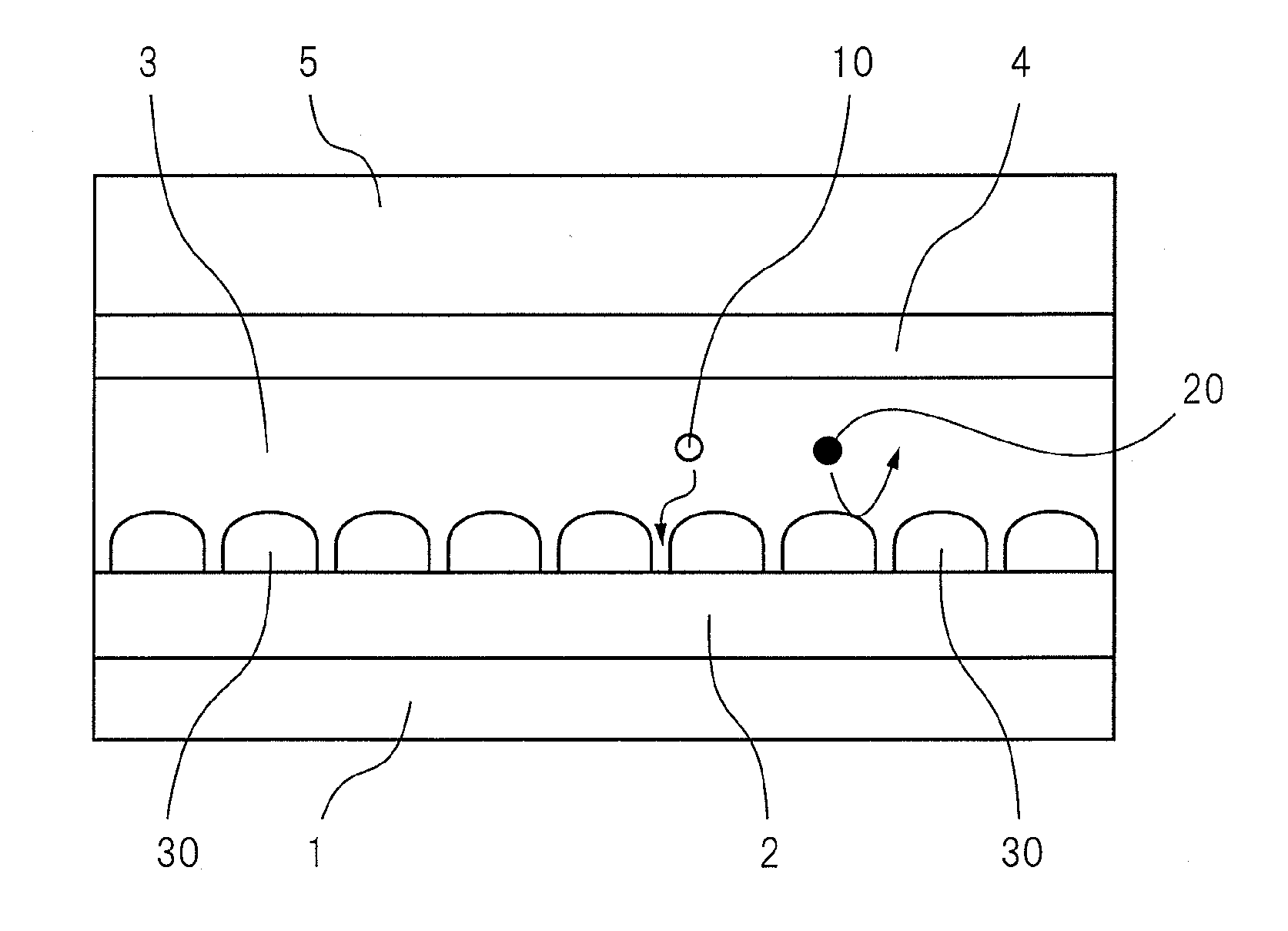
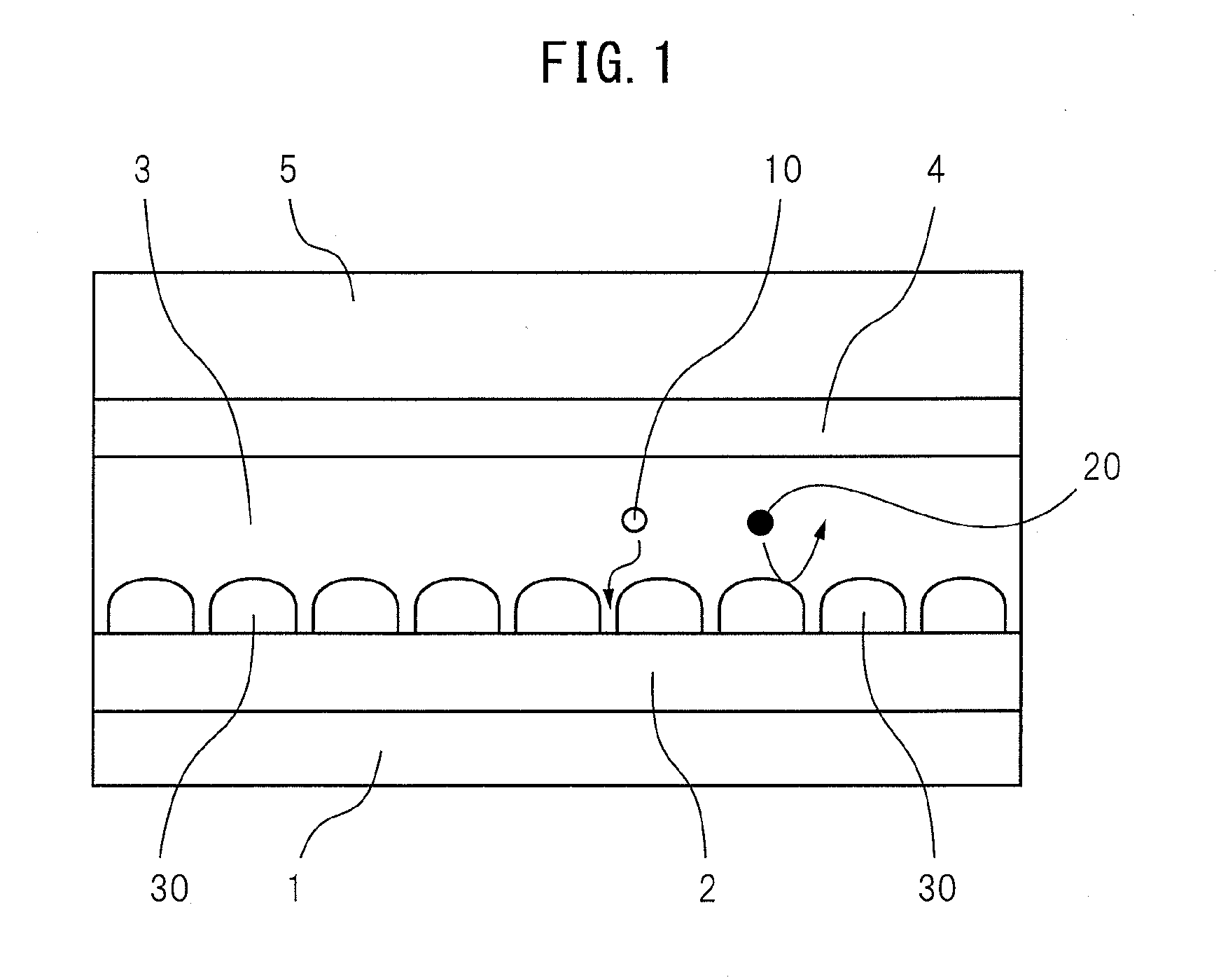
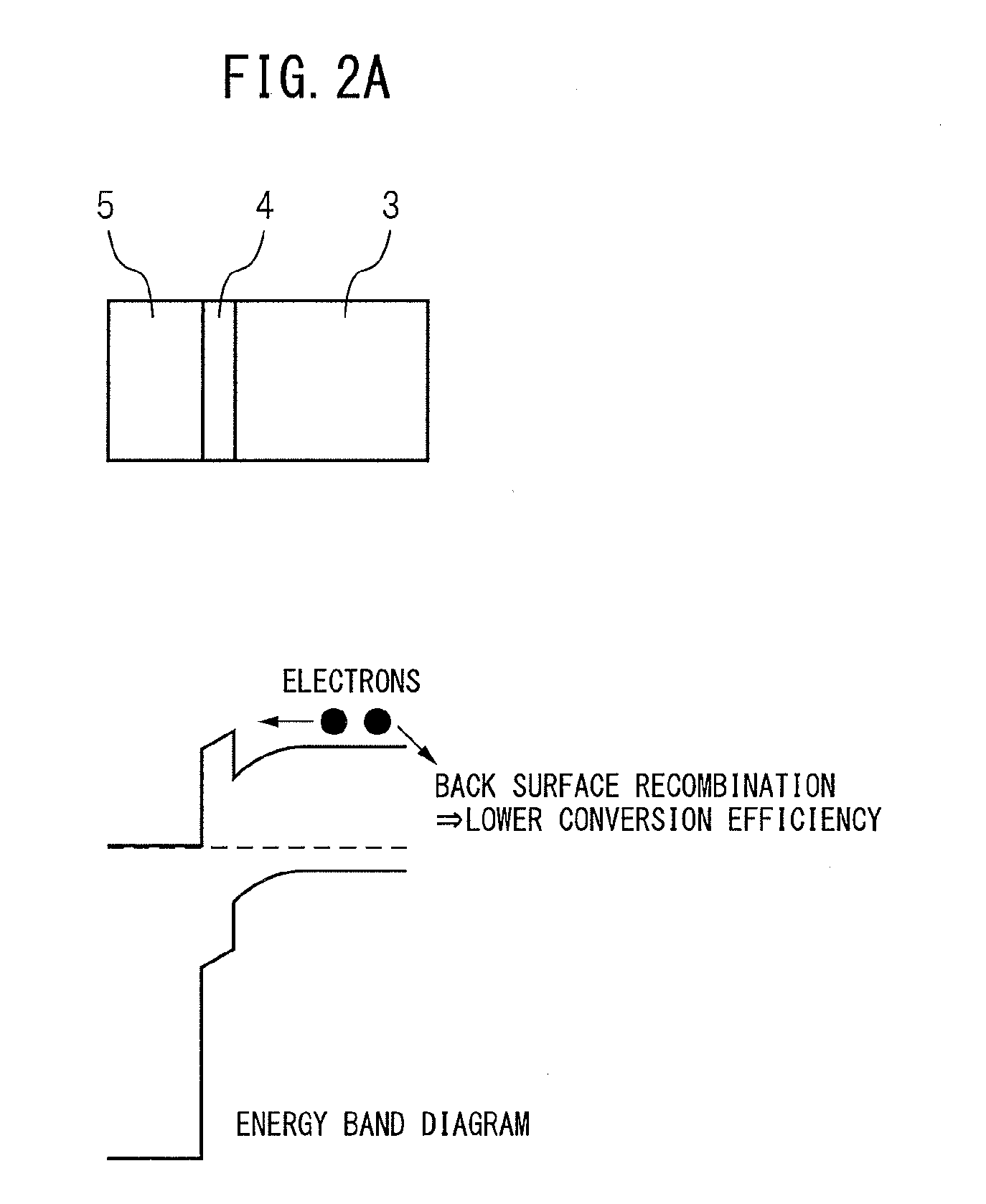
[0029]In general, the contact interface between the light absorption layer (semiconductor layer) and metal back electrode layer in a solar cell is a part which has a high density of dangling bonds and other crystal defects and where the speed of recombination of carriers becomes the fastest. Therefore, in a crystalline solar cell which is made using a conventional silicon wafer as a material, a point contact structure which uses a high quality passivation film is employed between the light absorption layer and the back electrode layer and reduction of the speed of recombination of carriers is sought.

[0030]However, in current CZTS-based thin film solar cells, realization of the point contact which is employed in crystalline solar cells is difficult. When applying the above art relating to crystalline silicon solar cells to a CZTS-based thin film solar cell, it is necessary to form a reduced defect, high quality insulating film (passivation film) between the semiconductor layer and el...


PUM

PropertyMeasurementUnit
sizeaaaaaaaaaa
temperatureaaaaaaaaaa
thicknessaaaaaaaaaa

Abstract

A CZTS-based thin film solar cell which has a high photovoltaic conversion efficiency which is provided with a substrate, a metal back electrode layer which is formed on the substrate, a p-type CZTS-based light absorption layer which is formed on the metal back electrode layer, and an n-type transparent conductive film which is formed on the p-type CZTS-based light absorption layer and which has a dispersed layer of ZnS-based fine particles at the interface between the p-type CZTS-based light absorption layer and the metal back electrode layer.

Description

CROSS REFERENCE TO RELATED APPLICATIONS[0001]This application is a U.S. National Phase patent application of PCT / JP2012 / 080347, filed on Nov. 22, 2012, which claims priority to Japanese Patent Application No. 2011-257893, filed on Nov. 25, 2011, each of which is hereby incorporated by reference in the present disclosure in its entirety.FIELD OF THE INVENTION[0002]The present invention relates to a CZTS-based thin film solar cell and a method of production of the same, more particularly relates to a CZTS-based thin film solar cell which has a high photovoltaic conversion efficiency and a method of production of the same.BACKGROUND OF THE INVENTION[0003]In recent years, thin film solar cells which use chalcogenide-based compounds generally called CZTS as the p-type light absorption layer have come under the spotlight. This type of solar cell is made of a relatively inexpensive material and has a band gap energy which is suitable for solar light, so holds forth the promise of inexpensi...

Claims


Application Information

Patent Timeline
Patent Type & Authority Applications(United States)
IPC IPC(8): H01L31/0224H01L31/0216H01L31/032
CPCH01L31/022425H01L31/02167H01L31/0324H01L31/0326H01L31/072H01L31/03845Y02E10/50
Inventor SUGIMOTO, HIROKIKATOU, TAKUYAMURAOKA, SATOSHI
Owner SOLAR FRONTIER
Why Eureka
Try Eureka