Image display device

a display device and image technology, applied in the field of image display devices, can solve the problems of increasing the cost of the vacuum envelope (the face panel and the back panel), and achieve the effects of simple structure, high dielectric strength and convenient manufacturing

Inactive Publication Date: 2005-09-22
PANASONIC LIQUID CRYSTAL DISPLAY CO LTD +1
View PDF6 Cites 40 Cited by
  • Summary
  • Abstract
  • Description
  • Claims
  • Application Information

AI Technical Summary

Benefits of technology

[0017] According to the present invention, a stem glass structural body, in which at least one conductive lead, which supplies a voltage from the outside, is embedded in the stem glass, and an exhaust pipe, which I used to evacuate the inside of the envelope and is integrally formed on a center portion thereof, are hermetically joined to at least one portion of the vacuum envelope; and, hence, it is possible to realize a conductive connection having a high dielectric strength property with a simple structure that is easy to manufacture, whereby the vacuum envelope can be realized at a low cost, thus giving rise to an excellent advantageous effect in that the manufacturing cost can be reduced.
[0018] Further, according to the present invention, by choosing an...

Problems solved by technology

However, the mounting of the anode button structure on an ordinary sheet of glass, which constitutes a back panel, is technically extremely difficult; and, hence, the back pa...

Method used


Image

  • Image display device
  • Image display device
  • Image display device

Examples


embodiment 1

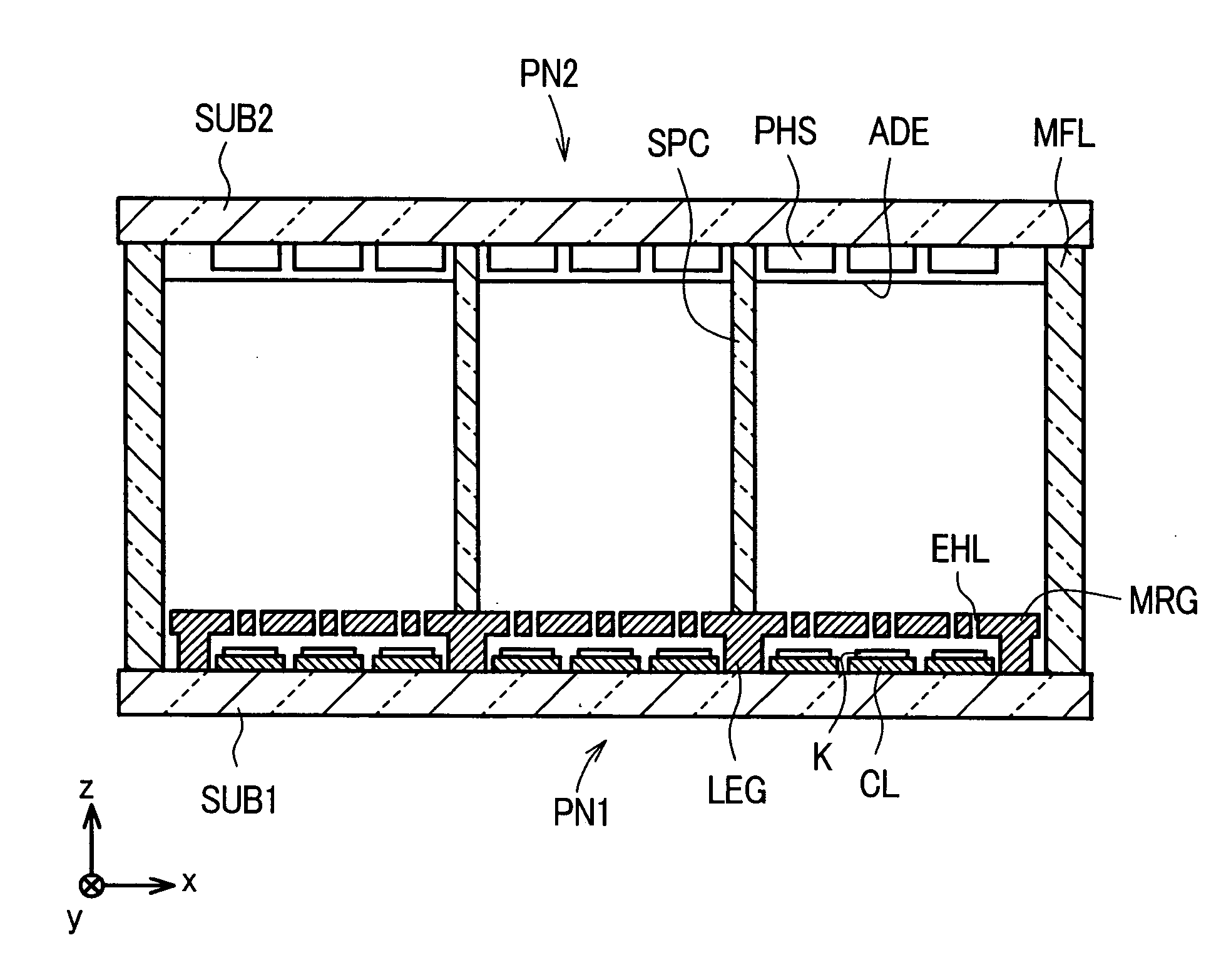
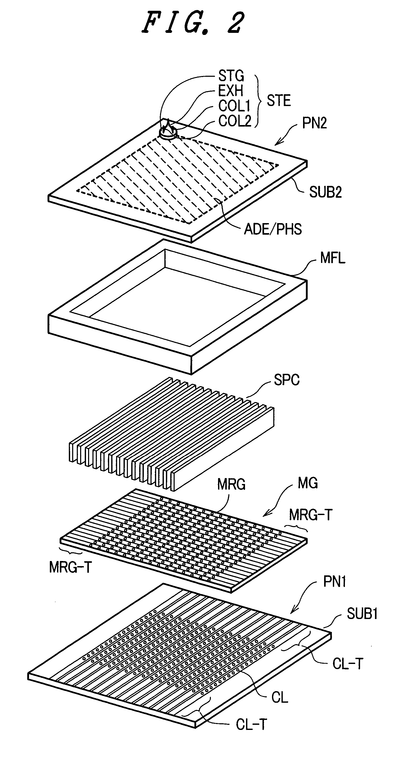
[0031]FIG. 1 is a cross-sectional view showing an embodiment 1 of an image display device of the present invention. In FIG. 1, SUB1 is a back substrate, which is formed as an insulating substrate, such as a glass plate, and it constitutes a back panel PN1. On an inner surface of the back substrate SUB1, a plurality of cathode lines CL are formed, which extend in one direction y (the horizontal direction) and are arranged in parallel in another direction x (vertical direction), and they include electron sources K, which use CNT (carbon nanotubes. Further, on the back panel PN1, control electrodes are arranged in the following manner. That is, a plurality of control electrode elements MRG, which cross the cathode lines CL in a non-contact manner, extend in the x direction and are arranged in parallel in the y direction, whereby pixels are formed at crossing portions with the cathode lines CL, and they have electron passing holes EHL, which allow electrons from the electron sources K t...

embodiment 2

[0049]FIG. 6 shows an embodiment 2 of an image display device according to the present invention, wherein parts identical with the parts shown in FIG. 3 are identified by the same symbols. Further, the cathode lines CL, the control electrode elements MRG and the like, which are formed on the back substrate SUB1, are omitted from the drawing. The constitution which makes this embodiment different from the embodiment shown in FIG. 3 lies in the fact that, in a corner portion of the back substrate SUB1, which constitutes the back panel PN1, outside of the display region, an opening OPN2 is formed, wherein a stem glass structural body STE having the same constitution as the stem glass structural body STE in FIG. 3 is hermetically joined to the opening OPN2 by welding with curing by heating. Here, in the stem glass structural body STE, a tip-off portion thereof is mechanically protected by a CRT socket made of an insulating resin material having an electrode terminal which is connected w...

embodiment 3

[0053]FIG. 7 shows an embodiment 3 of the image display device according to the present invention, wherein parts identical with the parts shown in FIG. 3 are identified by the same symbols. Also, in connection with this embodiment, illustration of the cathode lines CL, the control electrode elements MRG and the like, which are formed on the back substrate SUB1, is omitted from the drawing. The constitution which makes this embodiment shown in FIG. 7 different from the embodiment shown in FIG. 3 lies in the fact that, in a corner portion of the back substrate SUB1, which constitutes the back panel PN1, outside the display region, an opening OPN2 is formed, wherein a stem glass structural body STE, having the same constitution as the stem glass structural body STE in FIG. 3, is hermetically joined to the opening OPN2 by welding with curing by heating. Here, in the stem glass structural body STE, the tip-off portion is mechanically protected, by a CRT socket made of an insulating resin...


PUM


Abstract

In a corner portion outside a display region of a face substrate which constitutes a face panel of a display device, an opening is formed. In the opening, a stem glass structural body, which is configured by integrally forming an exhaust pipe on a center portion of a stem glass and by forming conductive leads in a peripheral portion thereof in an embedded manner, is fixed by welding using curing by heating. The exhaust pipe is evacuated and, thereafter, tipped off, thus realizing vacuum sealing of the inside thereof. A lead line is connected to a distal end of one conductive lead by welding and another end of the lead line is electrically connected with one end portion of the anode formed on an inner surface of the face substrate using a conductive adhesive agent. Further, a getter is mounted and fixed to another conductive lead line by welding.

Description

BACKGROUND OF THE INVENTION [0001] The present invention relates in general to an image display device of the type which includes electron beam sources having electron sources (cathodes) which emit electrons and phosphors, which are excited upon radiation by electron beams that are emitted from the electron sources toward anodes; and, more particularly, the invention relates to an image display device of the type described, which includes an improved voltage supply means that supplies a high voltage to the anodes. [0002] As a display device which exhibits a high brightness and high definition, color cathode ray tubes have been widely used for many years. However, along with the recent desire for images of higher quality in information processing equipment or television broadcasting, the demand for planar displays (panel displays) which are light in weight and require a small space, while exhibiting high brightness and high definition, has been increasing. As typical examples, liquid...

Claims


Application Information

Patent Timeline
IPC IPC(8): H01J1/62H01J29/90H01J29/86H01J31/12H01J63/04
CPCH01J29/90H01J29/94H01J2329/941H01J2217/49264H01J2329/90H01J31/123B65G33/08B65G47/56B09B3/40
Inventor NAKAMURA, TOMOKINOGUCHI, KAZUNARIKANEKO, YOSHIYUKI
Owner PANASONIC LIQUID CRYSTAL DISPLAY CO LTD
Why Eureka
Try Eureka