Monitoring the deposition properties of an oled

a technology of deposition properties and oleds, which is applied in the direction of discharge tube luminescnet screens, semiconductor/solid-state device testing/measurement, instruments, etc., can solve the problems of not being able to measure the actual films being deposited on the substrate, requiring frequent changes, and affecting the calibration accuracy. , to achieve the effect of improving the control of the deposition process, reducing the occurrence of devices, and improving manufacturing yield loss

Active Publication Date: 2005-09-22
GLOBAL OLED TECH
View PDF21 Cites 31 Cited by
  • Summary
  • Abstract
  • Description
  • Claims
  • Application Information

AI Technical Summary

Benefits of technology

[0006] It is another object of the present invention to improve control of the deposition process for the thin film, thereby reducing the occurrence of devices having sub-optimal device characteristics or improving manufacturing yield loss.

Problems solved by technology

This technique, however, has the disadvantage that the crystal mass sensor will have a large film build-up in a high volume mass production environment, which can alter the calibration over time and require frequent changing.
Another disadvantage is that the crystal mass sensor is located outside the area of the device and therefore must be calibrated to relate to the deposition on the substrate that is in a physically different location.
Therefore, this technique has the inherent disadvantage of not being able to measure the actual films being deposited on the substrate.
This method, however, still has the problem that the measurement device is outside the area of the substrate and requires cross calibration that can vary over time.
Inaccuracy of the calibration can result in the thickness of the film being different in the target that might result in sub-optimal device characteristics or manufacturing yield loss.

Method used


Image

  • Monitoring the deposition properties of an oled
  • Monitoring the deposition properties of an oled
  • Monitoring the deposition properties of an oled

Examples


Embodiment Construction

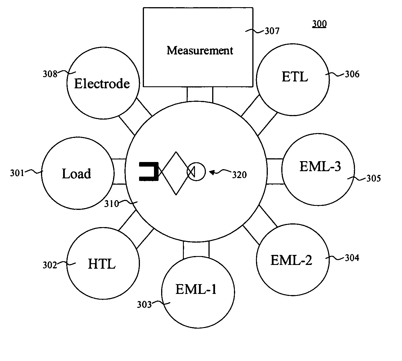
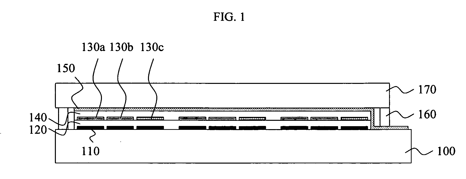
[0019] An OLED device is constructed by sandwiching two or more organic layers between a first and second electrode. In a passive matrix device, the first electrode is supplied on the device substrate forming laterally spaced rows. Alternately, in an active matrix device, thin film transistors, capacitors, and electrode lines are formed over the substrate and first electrode connections are formed on the substrate and are electrically connected to the active matrix circuitry.

[0020] Two or more organic layers are formed over the first electrode. For example, the OLED can be formed by first depositing a hole-transporting layer, then an emission layer, and finally an electron-transporting layer. The organic layers are typically deposited by using evaporation sources where the organic materials are heated such that vapor is produced and deposited on the substrate. The layers are typically deposited in vacuum chambers. Shadowmasks are used to control where on the substrates the organic ...


PUM

PropertyMeasurementUnit
pressureaaaaaaaaaa
pressureaaaaaaaaaa
vacuum pressureaaaaaaaaaa

Abstract

A method for making an OLED device includes providing a substrate having one or more test regions and one or more device regions, moving the substrate into a least one deposition chamber for deposition of at least one organic layer, and depositing the at least one organic layer through a shadowmask selectively onto the at least one device region and at least one test region on the substrate. The method also includes measuring a property of the at least one organic layer in the at least one test region, and adjusting the deposition process in accordance with the measured property.

Description

FIELD OF THE INVENTION [0001] The present invention relates generally to monitoring and controlling the formation of organic layers deposited in making organic light-emitting devices. BACKGROUND OF THE INVENTION [0002] Full color organic electroluminescent (EL), also known as organic light-emitting devices (OLED), have recently been demonstrated as a new type of flat panel display. In simplest form, an organic EL device is comprised of an electrode serving as the anode for hole injection, an electrode serving as the cathode for electron injection, and an organic EL medium sandwiched between these electrodes to support charge recombination that yields emission of light. An example of an organic EL device is described in U.S. Pat. No. 4,356,429. In order to construct a pixilated display device such as is useful, for example, as a television, computer monitor, cell phone display or digital camera display, individual organic EL elements can be arranged as an array of pixels in a matrix ...

Claims


Application Information

Patent Timeline
Patent Type & Authority Applications(United States)
IPC IPC(8): C23C14/04C23C14/54G01B11/06H01L51/40
CPCH01L51/0008H10K71/16
Inventor WINTERS, DUSTIN L.RICKS, MICHELE L.ARMSTRONG, NANCY J.CUPELLO, ROBERT S.
Owner GLOBAL OLED TECH
Why Eureka
Try Eureka