Interconnects with a dielectric sealant layer

a dielectric sealant and interconnect technology, applied in semiconductor devices, semiconductor/solid-state device details, electrical apparatus, etc., can solve the problems of reducing the performance limiting the fabrication of the integrated circuit, and the rejection rate due to the speed delay of the integrated circuit in the sub-micron regime has become a limiting factor, so as to reduce the parasitic rxc time delay, and reduce the conductive feature

Active Publication Date: 2005-09-22
ADVANCED MICRO DEVICES INC
View PDF5 Cites 47 Cited by
  • Summary
  • Abstract
  • Description
  • Claims
  • Application Information

AI Technical Summary

Benefits of technology

[0009] An advantage of the present invention is a method of manufacturing a semiconductor device exhibiting reduced parasitic RxC time delays comprising low-k dielectric materials, particular porous low-k dielectric materials, without barrier metal and / or barrier metal precursor penetration into the low-k material.
[0010] Another advantage of the present invention is a semiconductor device having interconnection patterns exhibiting reduced parasitic RxC time delays comprising low-k dielectric materials, particular porous low-k dielectric materials, without barrier metal and / or barrier metal precursor penetration into the low-k material.
[0011] Additional advantages and other features of the present invention will be set forth in the description which follows and in part will be apparent to those having ordinary skill in the art upon examination of the following or may be learned from the practice of the present invention. The advantages of the present invention may be realized and obtained as particularly pointed out in the appended claims.
[0012] According to the present invention, the foregoing and other advantages are achieved in part by a method of manufacturing a semiconductor device, the method comprising: forming an opening in a dielectric layer, comprising a low-k material having a pendant functional group, overlying a lower conductive feature, the opening defined by sidewalls of the low-k dielectric layer; depositing a sealant layer of a dielectric material on the sidewalls of the low-k dielectric layer, the dielectric material having a functional group which bonds to the pendant functional group of the low-k material; depositing a barrier metal layer lining the opening and on the sealant layer, and filling the opening with a conductive material, wherein the sealant layer prevents the barrier metal or a precursor used to deposit the barrier metal from penetrating the low-k material.
[0013] Embodiments of the present invention include forming a dual damascene opening in a porous, organosilicate low-k interlayer dielectric (ILD), the porous organosilicate comprising a pendant silanol functional group, depositing a siloxane polymer having a silylating functional group which reacts with the pendant silanol functional group of the organosilicate to form a sealant layer having a thickness from less than about 10 Å to about 100 Å, depositing a Ta and / or TaN barrier metal by CVD or ALD lining the opening and on the sealant layer, and filling the opening with Cu or Cu alloy. Embodiments of the present invention further include depositing a seedlayer on the barrier metal layer and filling the opening with Cu or Cu alloy by electroplating. Embodiments of the present invention also include conducting chemical-mechanical polishing (CMP) after depositing the Cu or Cu alloy, and then depositing a capping layer, such as silicon nitride or silicon carbide.
[0014] Another aspect of the present invention is a semiconductor device comprising: an interlayer dielectric (ILD), comprising a low-k material having a pendant functional group, overlying a lower conductive feature; an opening in the ILD overlying the lower conductive feature, the opening defined by sidewalls of the low-k material; a sealant layer on the side surfaces of the low-k material, the sealant layer comprising a dielectric material having a functional group bonded to the pendant functional group of the low-k material; a barrier metal layer lining the opening and on the sealant layer; and a conductive material filling the opening.

Problems solved by technology

Interconnection technology is constantly challenged to satisfy the ever increasing requirements for high density and performance associated with ultra large scale integration semiconductor devices.
The rejection rate due to integrated circuits speed delays in sub-micron regimes has become a limiting factor in fabrication.
However, Cu is a mid-gap impurity in silicon and silicon dioxide.
Accordingly, Cu diffusion through interlayer dielectrics, such as silicon dioxide, degrades the performance of the integrated circuit.
In attempting to employ various low-k materials, particularly porous low-k dielectric materials in interconnect technology, as for a dielectric layer in damascene techniques, various issues arise.
However, deposition precursors usually diffuse into such porous ILD materials and deposit metal in the pores throughout the ILD film, thereby causing leakage and capacitance degradation.
This problem is particularly acute in porous films where the pores are completely interconnected.
This problem may also occur when employing non-porous low-k materials in situations where the CVD or ALD precursors diffuse into the ILD material and are trapped, thereby causing leakage and capacitance degradation.

Method used


Image

  • Interconnects with a dielectric sealant layer
  • Interconnects with a dielectric sealant layer
  • Interconnects with a dielectric sealant layer

Examples


Embodiment Construction

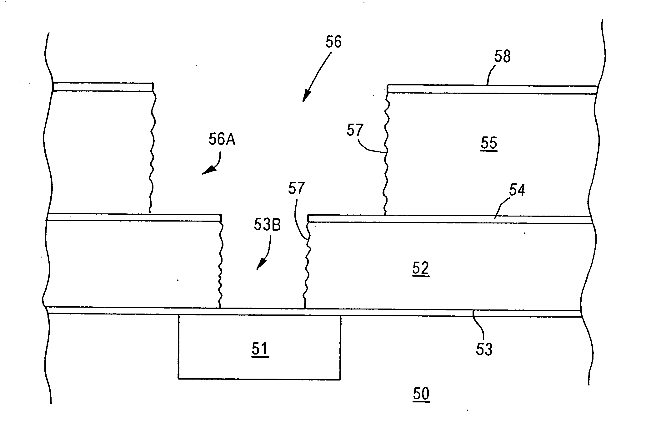
[0021] The present invention addresses the problem of barrier metal and / or barrier metal precursor penetration through sidewalls and into a low-k material during damascene processing, particularly porous low-k material. It was found that during CVD and ALD deposition of a thin conformal barrier metal layer, such as Ta and / or TaN, prior to the filling damascene openings with Cu or a Cu alloy, the barrier metal and / or precursor penetrated through the sidewalls of the low-k dielectric layer. Such penetration was particularly acute in implementing damascene processing employing porous low-k materials, such as porous low-k dielectric material having a dielectric constant (k) less than about 2.5. Such penetration into the low-k material causes leakage and capacitance degradation. This problem is not confined to porous low-k material, but may also occur with non-porous low-k material by diffusion of the barrier metal and / or barrier metal precursor through the exposed sidewalls into the low...


PUM

PropertyMeasurementUnit
porosityaaaaaaaaaa
dielectric constantaaaaaaaaaa
temperaturesaaaaaaaaaa

Abstract

Leakage, capacitance and reliability degradation of interconnects fabricated in low-k dielectric materials, particularly porous low-k dielectric material, due to penetration by a barrier metal and / or barrier metal precursor during damascene processing is prevented by depositing a conformal, heat stable dielectric sealant layer on sidewalls of the low-k dielectric material defining the damascene opening. Embodiments include forming a dual damascene opening in a porous, low-k organosilicate layer, the organosilicate having a pendant silanol functional group, depositing a siloxane polymer having a silylating functional group which bonds with the pendant silanol group to form the sealant layer, depositing a Ta and / or TaN barrier metal layer by CVD or ALD and filling the opening with Cu or a Cu alloy.

Description

FIELD OF THE INVENTION [0001] The present invention relates to a method of manufacturing a semiconductor device exhibiting increased operating speed and improved reliability. The present invention has particular applicability in manufacturing high density, multi-level semiconductor devices comprising sub-micron dimensioned interconnects formed with high precision and improved reliability. BACKGROUND ART [0002] Interconnection technology is constantly challenged to satisfy the ever increasing requirements for high density and performance associated with ultra large scale integration semiconductor devices. The speed of semiconductor circuitry varies inversely with the resistance (R) and capacitance (C) of the interconnection system. The higher the value of the R x C product, the more limiting the circuit speed. As integrated circuits become complex and feature sizes and spacings become smaller, the integrated circuit speed becomes less dependent upon the transistor itself and more dep...

Claims


Application Information

Patent Timeline
Patent Type & Authority Applications(United States)
IPC IPC(8): H01L21/4763H01L21/768H01L23/48H01L23/52H01L23/522H01L23/532H01L29/40
CPCH01L21/76807H01L21/7682H01L21/76831H01L23/53295H01L23/53238H01L23/5329H01L23/5226H01L2221/1047H01L2924/0002H01L2924/00
Inventor RYAN, E. TODD
Owner ADVANCED MICRO DEVICES INC
Why Eureka
Try Eureka