CMP process control method

a technology of process control and control method, which is applied in the direction of electric programme control, lapping machines, manufacturing tools, etc., can solve the problems of poor lithography, window-etching or plug-formation difficulties, and the difficulty of controlling the polishing rate of the cmp process at different locations on the wafer surfa

Active Publication Date: 2005-09-22
TAIWAN SEMICON MFG CO LTD
View PDF13 Cites 14 Cited by
  • Summary
  • Abstract
  • Description
  • Claims
  • Application Information

AI Technical Summary

Benefits of technology

[0025] In accordance with these and other objects and advantages, the present invention generally relates to an improved, one-time feedback CMP process control method which contributes to uniformity in the quantity of material removed from wafers in a lot during semiconductor processing and is suitable for complex processes such as STI (shallow trench isolation) fabrication procedures. According to one embodiment of the method, a pre-CMP thickness of each of multiple pilot wafers in a wafer lot is initially measured. The pilot wafers are then polished according to a default or given process recipe having a process time which is ordinarily used for the CMP process. After the CMP polishing sequence is completed, the post-CMP thickness of each pilot wafer is measured. Both the divergence of the post-CMP thickness of each wafer from a target thickness and the material removal rate of each polishing head in the apparatus are then determined.

Problems solved by technology

The amount of the dielectric material removed is normally between about 2000 A and about 10,000 A. The uniformity requirement for STI, ILD or IMD polishing is very stringent since non-uniform dielectric films lead to poor lithography and resulting window-etching or plug-formation difficulties.
While the CMP process provides a number of advantages over the traditional mechanical abrasion type polishing process, a serious drawback for the CMP process is the difficulty in controlling polishing rates at different locations on a wafer surface.
However, the continuous feedback mechanism is unsuitable for more complex processes, such as STI (shallow trench isolation) CMP processes.
Use of the single-variable continuous feedback mechanism in an STI CMP process frequently causes over-prediction and over-adjustment to the material removal rate for succeeding wafers in a lot.

Method used


Image

  • CMP process control method
  • CMP process control method
  • CMP process control method

Examples


Embodiment Construction

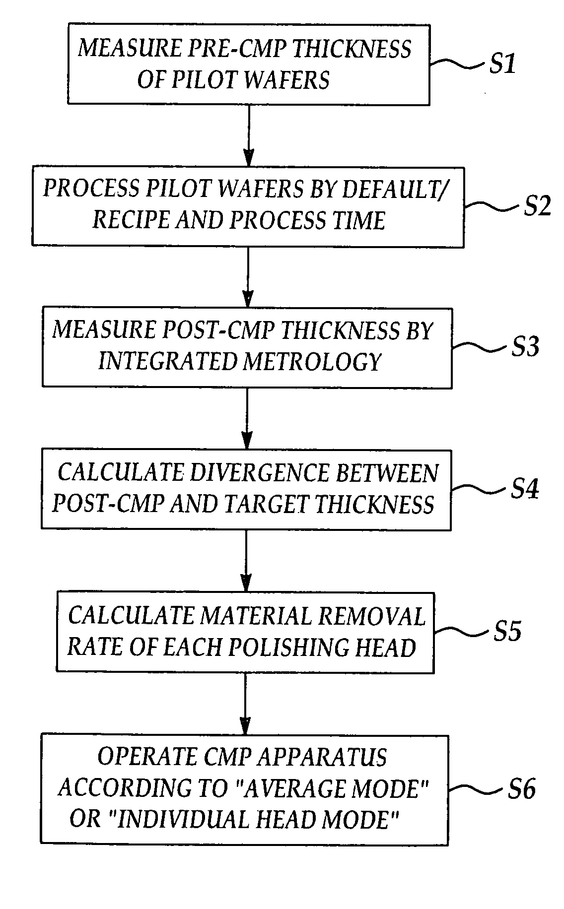
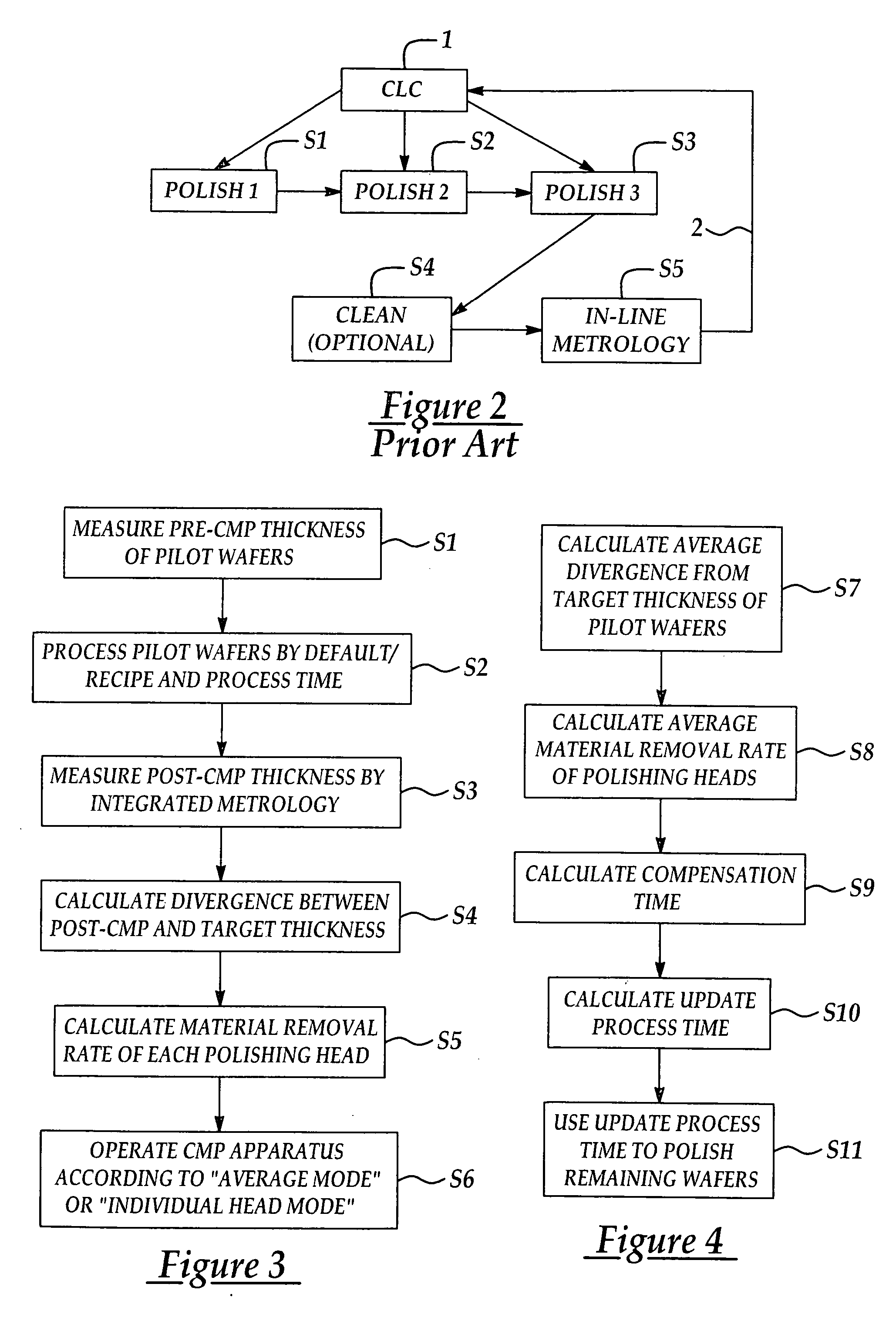
[0043] The present invention contemplates a one-time feedback CMP process control method which is used to polish each of successive wafers in one or more wafer lots, typically in the fabrication of semiconductor integrated circuits on the wafers. The method includes a one-time, rather than a continuous, feedback or update polish time adjustment to the polishing heads on the CMP apparatus for each of the successive wafers in the wafer lot. The update polish time adjustment is first obtained by processing multiple pilot wafers and is then used to polish the remaining wafers in the lot or in successive lots. The method contributes to uniformity in the quantity of material removed from wafers in a wafer lot during chemical mechanical polishing of the wafers. The method is suitable for complex processes such as STI (shallow trench isolation) fabrication procedures, for example.

[0044] Referring to FIG. 6, the one-time feedback CMP process control method of the present invention is carrie...


PUM

PropertyMeasurementUnit
thicknessaaaaaaaaaa
thicknessaaaaaaaaaa
thicknessaaaaaaaaaa

Abstract

A one-time feedback CMP process control method which contributes to uniformity in the quantity of material removed from wafers in a lot during semiconductor processing and is suitable for complex processes such as STI (shallow trench isolation) fabrication procedures, is disclosed. The method includes providing a plurality of wafers having a set of pilot wafers and a set of remaining wafers, polishing each of the pilot wafers according to an original process time, determining a compensation time for the pilot wafers, determining an update time by adding the compensation time to the original process time and polishing the set of remaining wafers according to the update time.

Description

FIELD OF THE INVENTION [0001] The present invention relates to chemical mechanical polishing apparatus for polishing semiconductor wafer substrates. More particularly, the present invention relates to an improved CMP process control method which includes a one-time polishing time feedback adjustment for all wafers in a lot to facilitate greater between-wafer uniformity in the quantity of material removed from the wafers in a CMP process. BACKGROUND OF THE INVENTION [0002] In the fabrication of semiconductor devices from a silicon wafer, a variety of semiconductor processing equipment and tools are utilized. One of these processing tools is used for polishing thin, flat semiconductor wafers to obtain a planarized surface. A planarized surface is highly desirable on a shadow trench isolation (STI) layer, inter-layer dielectric (ILD) or on an inter-metal dielectric (IMD) layer, which are frequently used in both memory and logic devices. The planarization process is important since it e...

Claims


Application Information

Patent Timeline
Patent Type & Authority Applications(United States)
IPC IPC(8): B24B37/04B24B49/00B24B51/00G05B19/04H01L21/304
CPCB24B49/00B24B37/042
Inventor CHEN, CHEN-SHIENHUANG, YAI-YEICHEN, YEAN-ZHAWCHEN, KAI-HSIUNGLIN, YIH-SHUNG
Owner TAIWAN SEMICON MFG CO LTD
Why Eureka
Try Eureka