Method and system for analyzing defects of an integrated circuit wafer

a technology of integrated circuit and defect analysis, which is applied in the direction of individual semiconductor device testing, semiconductor/solid-state device testing/measurement, instruments, etc., can solve the problems of deteriorating the performance of the semiconductor device, severe damage to the semiconductor circuit, and loss of yield, so as to achieve high yield-killing defects and efficient analysis of visual defects

Active Publication Date: 2005-09-22
MACRONIX INT CO LTD
View PDF4 Cites 20 Cited by
  • Summary
  • Abstract
  • Description
  • Claims
  • Application Information

AI Technical Summary

Benefits of technology

[0010] Roughly described, one aspect of the present invention relates to providing a system and method for efficiently analyzing visual defects of a semiconductor wafer having integrated circuit semiconductor dice thereon in the manufacturing process by utilizing an asymmetric visual defect review methodology which emphasizes high yield-killing defects out of numerous reported defects within limited review capacity and manpower.
[0011] The present invention provides an effective defect review method. As a result, the present invention efficiently and effectively analyzes the visual defects of a semiconductor wafer in the manufacturing process.

Problems solved by technology

Defects are the major “killers” of devices formed during manufacturing, resulting in yield loss.
It is believed that the visual defects with larger defect size have greater “killing power” and will cause severe damage on the semiconductor circuit and deteriorate the performance of the semiconductor device.
The design rules of devices have been rapidly shrinking.
Most defects found visually, however, are not yield-killing.
But no good automated method has been found yet for reliably determining which preliminary defects are yield killers and which are not.
The review step is expensive, however, both because the review station equipment is expensive and because the time required for human review of a defect is substantial.
But the operator could not otherwise specify that the selection was to emphasize defects having a larger size.
This sampling algorithm was therefore doubly-deficient: not only did it fail to emphasize the types of defects that were more likely to be yield killers, but because the number of defects of each size typically decreases rapidly as the size increases, a random sampling in which each defect is given equal likelihood of selection regardless of its size would in fact greatly emphasize smaller defects, which are less likely to be yield killers.
Much time and expense has therefore in the past been used unproductively by obtaining redundant information from reviewing numerous small defects, while missing potentially important information that could be obtained by reviewing more larger-size defects.

Method used


Image

  • Method and system for analyzing defects of an integrated circuit wafer
  • Method and system for analyzing defects of an integrated circuit wafer
  • Method and system for analyzing defects of an integrated circuit wafer

Examples


Embodiment Construction

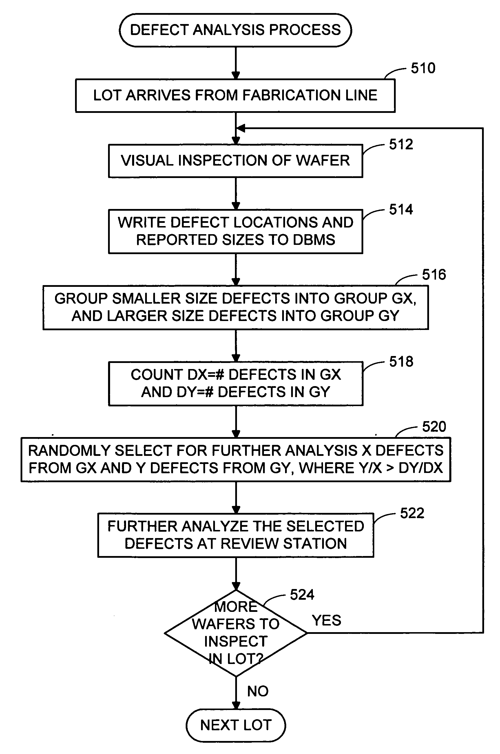
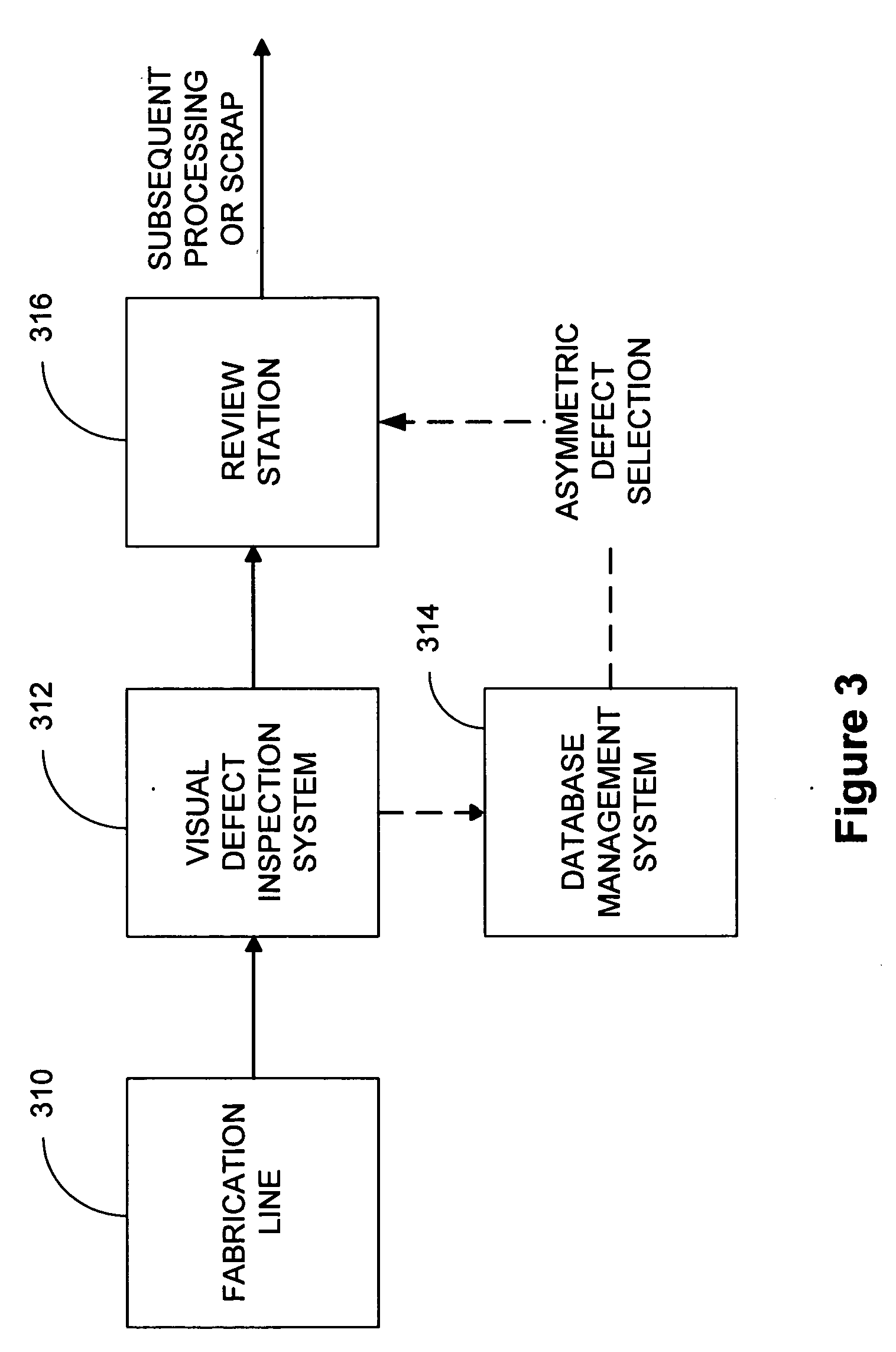
[0024] One purpose of the invention is to provide a method of efficiently analyzing visual defects of a semiconductor wafer in the manufacturing process. In an embodiment described herein, a wafer that has been subjected to (or will be subjected to) an integrated circuit manufacturing process, is first inspected by automated equipment to identify “preliminary” defects on the wafer. Typically the preliminary inspection is a machine-vision inspection, and is intended to detect all defects above a preset threshold, that are (or will be) located on integrated circuit dice. The preliminary inspection system reports at least a size and a location for each defect identified. The defects are then classified into at least two groups: a first group containing only defects having a reported size that is at least as small as a predetermined size typically specified by the operator, and a second group containing only defects having a reported size that is at least as large as the predetermined s...


PUM


Abstract

Method and apparatus for efficiently analyzing visual defects of an integrated circuit wafer in the manufacturing process thereof by utilizing an asymmetric visual defect review methodology that can effectively extract high yield-killing defects out of numerous reported defects within the limited capacity and manpower available for review. Roughly described, the method comprises inspecting the semiconductor wafer, thereby obtaining the defect location and defect size, sampling the defects asymmetrically by determining asymmetrical defect review ratios, and thereby reviewing the defects asymmetrically. Also described is a method of asymmetrically sampling visual defects that can effectively extract out high yield-killing defects from a mass of defects by determining asymmetric defect review ratios, and a system for use in sampling visual defects asymmetrically.

Description

BACKGROUND [0001] 1. Field of the Invention [0002] The present invention relates in general to semiconductor wafer manufacturing. More particularly, the present invention relates to analyzing visual defects of a semiconductor wafer by utilizing an asymmetric review methodology in the manufacturing process of the semiconductor wafer. [0003] 2. Description of Related Art [0004] Manufacturing processes for submicron integrated circuits (ICs) require strict process control for minimizing defects on integrated circuits. Defects are the major “killers” of devices formed during manufacturing, resulting in yield loss. Along with the trend of miniaturization of devices, the tolerance of defect size in IC chips becomes more stringent. Visual defect analysis has become an essential part of IC manufacturing processes. In-line inspection and review are important for determining whether wafers have become contaminated with particles due to a tool malfunction or process problem. [0005] It is belie...

Claims


Application Information

Patent Timeline
Patent Type & Authority Applications(United States)
IPC IPC(8): G06F17/50H01L21/00H01L21/66
CPCH01L22/20H01L22/12
Inventor LIAO, SHU-SINGMA, SZU-TSUN
Owner MACRONIX INT CO LTD
Why Eureka
Try Eureka