Techniques to reduce substrate cross talk on mixed signal and RF circuit design

a mixed signal and circuit design technology, applied in the direction of semiconductors, electrical devices, transistors, etc., can solve the problems of reducing the performance reducing the rf signal at such frequencies, and shrinking the spacing between the devices of the integrated circuit, etc., to achieve the effect of low resistivity

Inactive Publication Date: 2005-09-29
HONEYWELL INT INC
View PDF11 Cites 48 Cited by
  • Summary
  • Abstract
  • Description
  • Claims
  • Application Information

AI Technical Summary

Benefits of technology

[0012] According to still another aspect of the present invention, a method of isolating a semiconductor feature of an integrated circuit from RF signals comprises the following: forming a buried insulation layer over a semiconductor substrate; forming a semiconductor feature in one or more semiconductor layers so that the semiconductor feature is formed over a portion of the buried insulation layer, wherein the buried insulating layer has a trench therethrough down to the semiconductor substrate that substantially encloses the portion o...

Problems solved by technology

This trend means that the spacing between devices of an integrated circuit shrinks.
As the spacing between devices shrinks, adjacent devices increasingly interact with each other, reducing performance of the integrated circuit.
RF signals at such frequencies are difficult to generate and control.
These signals also have a tendency to interfere with one other because they are easily coupled by parasitic properties present in all electronic components, including integrated circuits.
Such undesirable parasitic effects result, for example, from the conductive silicon substrates on which integrate...

Method used


Image

  • Techniques to reduce substrate cross talk on mixed signal and RF circuit design
  • Techniques to reduce substrate cross talk on mixed signal and RF circuit design
  • Techniques to reduce substrate cross talk on mixed signal and RF circuit design

Examples


Embodiment Construction

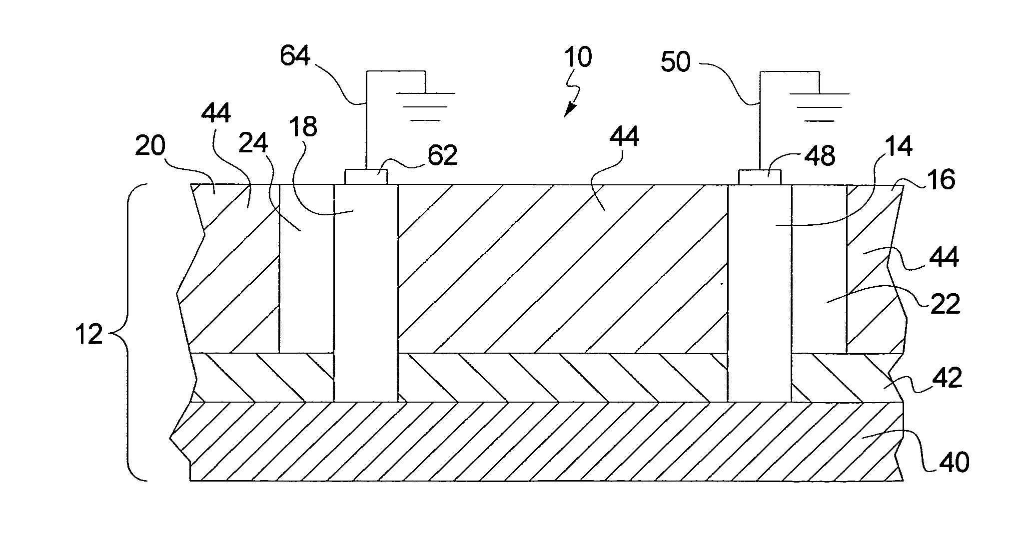
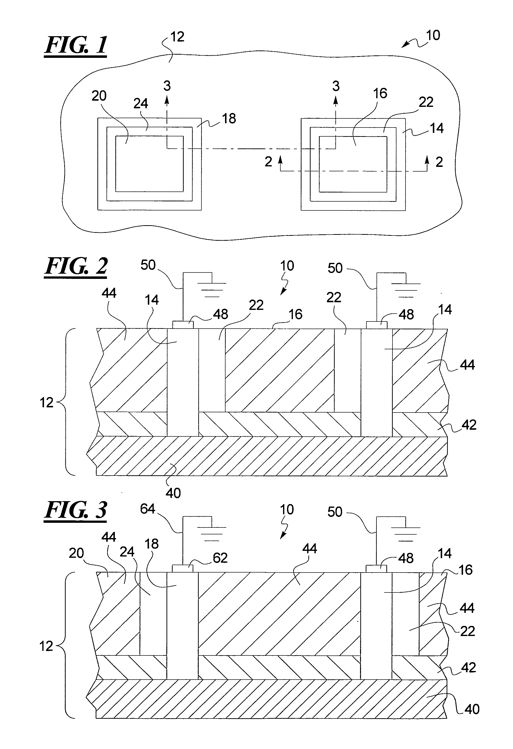
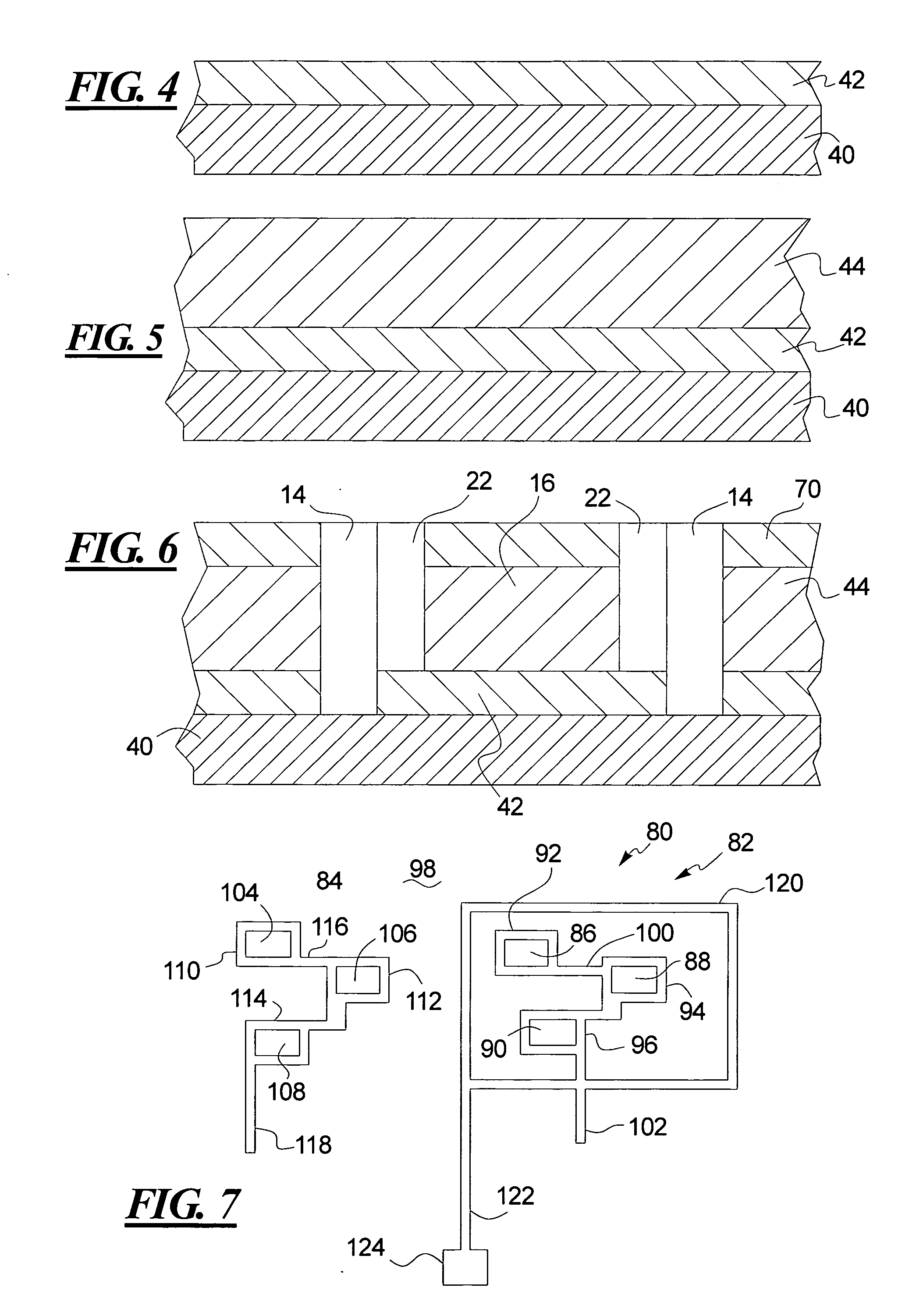
[0020] As shown in FIG. 1, a semiconductor integrated circuit 10 in accordance with one embodiment of the present invention includes a single SOI substrate 12. The SOI substrate 12 typically includes a silicon handle wafer, a buried oxide layer over the silicon handle wafer, and one or more silicon layers that are over the buried oxide layer and that are processed to form electronic devices of the integrated circuit. However, the present invention can be applied to non-SOI substrates, such as bulk silicon, and to other SOI substrates, such as SOS (silicon-on-sapphire) substrates.

[0021] The SOI substrate 12 includes a first isolation guard ring 14 that isolates a first device mesa 16 and a second isolation guard ring 18 that isolates a second device mesa 20. In addition, an optional first dielectric ring 22 may be provided between the first isolation guard ring 14 and the first device mesa 16, and an optional second dielectric ring 24 may be provided between the second isolation gua...


PUM


Abstract

An integrated circuit has a buried insulation layer formed over a semiconductor substrate, and a semiconductor mesa formed over the buried insulation layer. A low resistivity guard ring substantially surrounds the semiconductor mesa and is in contact with the semiconductor substrate. The low resistivity guard ring is grounded and isolates the semiconductor mesa from RF signals.

Description

TECHNICAL FIELD OF THE INVENTION [0001] The present invention relates to RF isolation in integrated circuits. BACKGROUND OF THE INVENTION [0002] It is well known that the general trend in semiconductor integrated circuit fabrication is to produce smaller and smaller devices so that more circuitry can be packed into less wafer real estate. This trend means that the spacing between devices of an integrated circuit shrinks. As the spacing between devices shrinks, adjacent devices increasingly interact with each other, reducing performance of the integrated circuit. [0003] The basic measurement parameter that characterizes this interaction effect is called electrical isolation. If high electrical isolation, and in particular, high RF isolation, between devices of an integrated circuit can be achieved, those devices can be spaced more closely together. As a result, the die size of the integrated circuit can be is minimized. Minimum size, in turn, implies smaller packaging and, thus, less...

Claims


Application Information

Patent Timeline
IPC IPC(8): H01L21/762H01L21/765
CPCH01L21/76283H01L27/1203H01L21/84H01L21/765
Inventor YUE, CHEISAN J.SEEFELDT, JAMES D.
Owner HONEYWELL INT INC
Why Eureka
Try Eureka